In the class, it is mentioned that single processor has reached the heat limit, the power density limit. I wonder, why don't we just make the processor's size larger while enhancing the frequency. The power density would then remain the same and the processor would achieve better performance.
bpr
@rehn1992, here are two problems with increasing the size of the processor:
1) the speed of light - at 2GHz, light can travel ~15cm per cycle. Signals travel slower than the speed of light.
2) yield - the larger the wafer / more transistors the increased chance that something will fail to fabricate.
anon
Is it possible that our current method of just adding new cores will also reach the power wall, or does this method allow for us to continually add cores without ever having to worry about a heat dissipation limit?
taobingxue
This method wouldn't allow us to add infinite cores. Even we have multi-cores, all these cores are on the same chip, otherwise, we need things like buses to communicate which cost more and is much more complicated. On one chip, due to the limitation of integration, we can't add infinite cores. At the same time, when there are too many cores, communication between two cores will increase.
ferozenaina
In the last few years, Intel moved from 22nm fabrication process to the 14nm for the Skylake processor. And it is expected to reach 10nm in Ice Lake 2018.
This increase in transistor density increases performance while still retaining the power dissipation. Is there further potential for miniaturizing the circuits?
I also understand that below a certain silicon width, we can't run the clocks at GHz due to interference.
petrichor
Wikipedia actually has a page dedicated to the physical limit to silicone fabrication feature size: https://en.wikipedia.org/wiki/5_nanometer (If you look on the right hand bar you can go through all the silicon fab sizes we've ever made chips with). The physical limit we reach at this scale is actually quantum tunneling effects whereby electrons can actually tunnel across the transistor even when it is in its non conducting state. Also just so you appreciate the scales we're talking about here, for pure crystalline silicon, the lattice spacing is about 0.5nm so a 5nm feature size corresponds to only 10 atoms of silicon! And our current 14nm process is only 28 atoms of silicon! Another interesting practical problem is performing lithography for such small features is a huge challenge considering that the wavelength of light that corresponds to 14nm is in the extreme ultra violet, which is absorbed by most normal glass optics, and going to 5nm, you start pushing into x-rays.
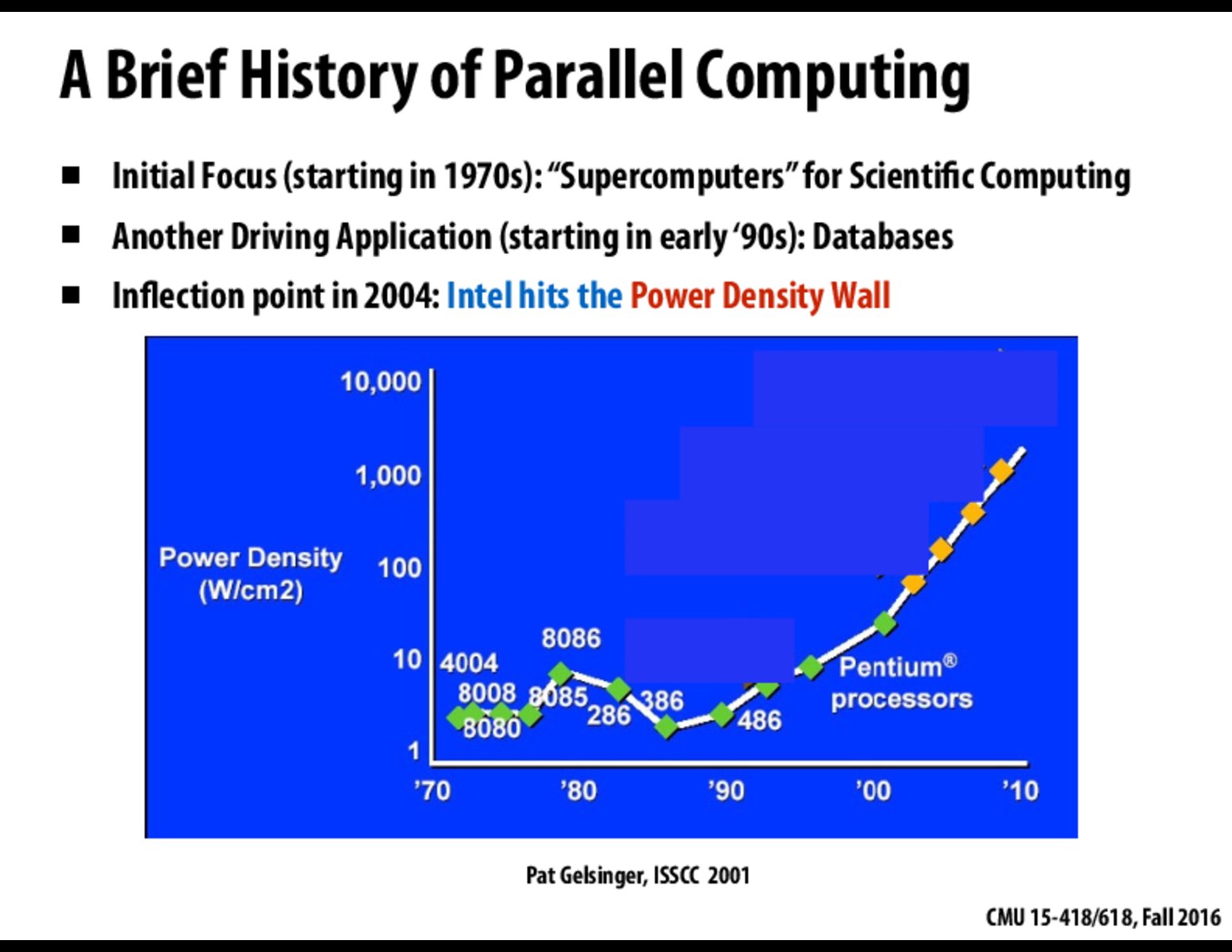
In the class, it is mentioned that single processor has reached the heat limit, the power density limit. I wonder, why don't we just make the processor's size larger while enhancing the frequency. The power density would then remain the same and the processor would achieve better performance.
@rehn1992, here are two problems with increasing the size of the processor: 1) the speed of light - at 2GHz, light can travel ~15cm per cycle. Signals travel slower than the speed of light.
2) yield - the larger the wafer / more transistors the increased chance that something will fail to fabricate.
Is it possible that our current method of just adding new cores will also reach the power wall, or does this method allow for us to continually add cores without ever having to worry about a heat dissipation limit?
This method wouldn't allow us to add infinite cores. Even we have multi-cores, all these cores are on the same chip, otherwise, we need things like buses to communicate which cost more and is much more complicated. On one chip, due to the limitation of integration, we can't add infinite cores. At the same time, when there are too many cores, communication between two cores will increase.
In the last few years, Intel moved from 22nm fabrication process to the 14nm for the Skylake processor. And it is expected to reach 10nm in Ice Lake 2018.
This increase in transistor density increases performance while still retaining the power dissipation. Is there further potential for miniaturizing the circuits?
I also understand that below a certain silicon width, we can't run the clocks at GHz due to interference.
Wikipedia actually has a page dedicated to the physical limit to silicone fabrication feature size: https://en.wikipedia.org/wiki/5_nanometer (If you look on the right hand bar you can go through all the silicon fab sizes we've ever made chips with). The physical limit we reach at this scale is actually quantum tunneling effects whereby electrons can actually tunnel across the transistor even when it is in its non conducting state. Also just so you appreciate the scales we're talking about here, for pure crystalline silicon, the lattice spacing is about 0.5nm so a 5nm feature size corresponds to only 10 atoms of silicon! And our current 14nm process is only 28 atoms of silicon! Another interesting practical problem is performing lithography for such small features is a huge challenge considering that the wavelength of light that corresponds to 14nm is in the extreme ultra violet, which is absorbed by most normal glass optics, and going to 5nm, you start pushing into x-rays.