I think I understand what L3 line unshared, shared line in another core, and modified in another core mean, but what does remote L3 CACHE refer to in terms of hardware?
kayvonf
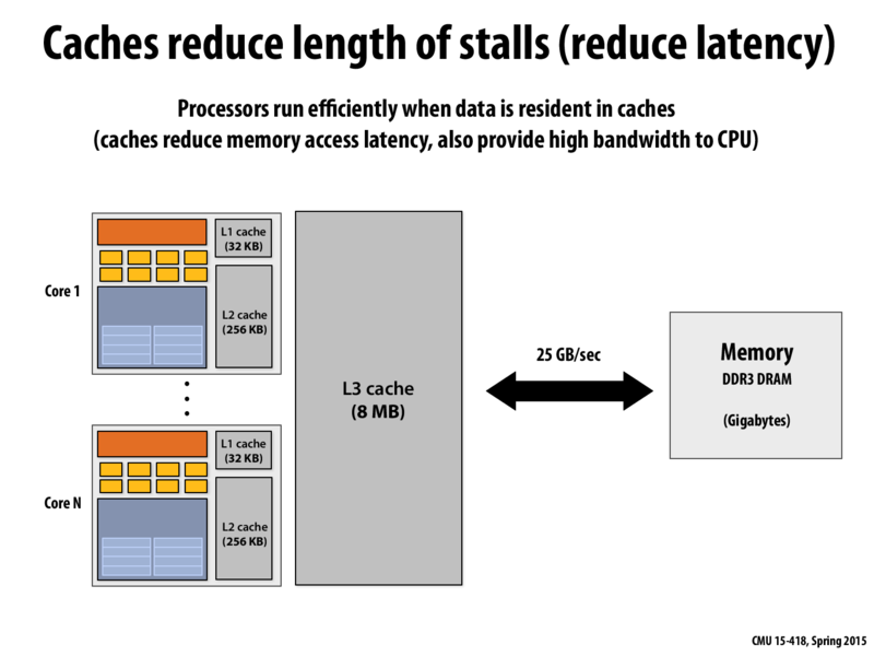
@yuel1: In Intel's modern "Core" architecture, the L3 cache, although it is a logically shared cache assessable by all cores as drawn here, the L3 cache SRAM is physically partitioned among the cores (implementation detail). Therefore, the L3 cache has non-uniform access characteristics. In a quad-core chip, that 8MB L3 is made up of 4 2MB slices (or "banks") in each of the cores. A processor's L3 hit latency is lower if the address is in the local slice of the L3. It's a very modular design.
yuel1
@kayvonf: I think I was a little vague in my question. What struck me as odd was the remote L3 Cache that took 100~300 cycles. Is that in reference to L3 cache slices that are not immediate neighbors of each other?
https://software.intel.com/en-us/forums/topic/287236
Take Intel i7 for an example. Here are the approximate latencies to access L1, L2, L3 caches and main memory:
L1 CACHE hit, ~4 cycles
L2 CACHE hit, ~10 cycles
L3 CACHE hit, line unshared ~40 cycles
L3 CACHE hit, shared line in another core ~65 cycles
L3 CACHE hit, modified in another core ~75 cycles
remote L3 CACHE ~100-300 cycles
Is more levels of cpu cache design simply better? Will we see a L4 cache appear in the future?
Found this on the internet:- http://hardware.slashdot.org/story/13/11/23/0137253/intels-128mb-l4-cache-may-be-coming-to-broadwell-and-other-future-cpus
I think I understand what L3 line unshared, shared line in another core, and modified in another core mean, but what does remote L3 CACHE refer to in terms of hardware?
@yuel1: In Intel's modern "Core" architecture, the L3 cache, although it is a logically shared cache assessable by all cores as drawn here, the L3 cache SRAM is physically partitioned among the cores (implementation detail). Therefore, the L3 cache has non-uniform access characteristics. In a quad-core chip, that 8MB L3 is made up of 4 2MB slices (or "banks") in each of the cores. A processor's L3 hit latency is lower if the address is in the local slice of the L3. It's a very modular design.
@kayvonf: I think I was a little vague in my question. What struck me as odd was the remote L3 Cache that took 100~300 cycles. Is that in reference to L3 cache slices that are not immediate neighbors of each other?