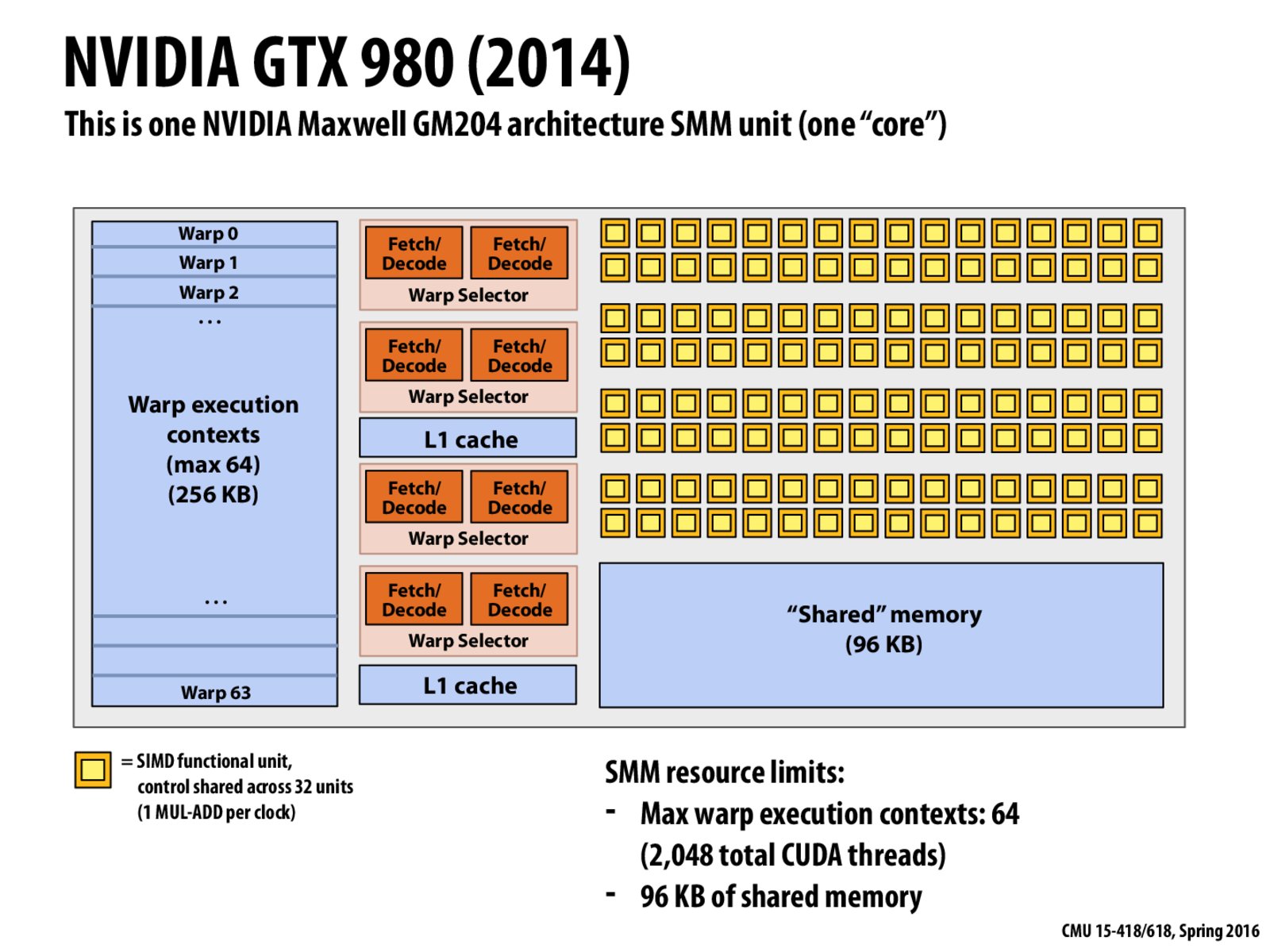
1) If we only have four 32-wide SIMD ALUs, why are there 64 warp spaces? That seems to me like a wide skew between the number of instructions streams that can be run at once (which is 4 from the above image), versus the number of execution contexts (warps) present in this core (64 from the above image)?
2) Where is the actual instruction stream (kernel) stored on this device? Or any GPU in general? Is it on chip, or fetched from host memory?
IntergalacticPeanutMaker
The instructions are stored in global memory that is inaccessible to the user but are prefetched into an instruction cache during execution.
The maximum kernel size is stated in the Programming Guide in section G.1: 2 million instructions.
@fleventyfive. Don't confuse the number of active warps on a core with the number of instructions that can be executed simultaneously. The core maintains storage for 64 warp execution contexts (equivalently 2048 CUDA thread contexts). However it can only run instructions from up to four warps simultaneously in any one clock. This is the idea of hardware multi-threading discussed earlier in the class. Where each warp has a nice analog to a hardware thread in an Intel CPU.
Question to anyone: And what was the motivation for hardware multi-threading?
BensonQiu
@kayvonf: We can use hardware multi-threading to hide memory stalls, as described in lecture 2, slide 52
.
rajul
I understand that there are 64 warp spaces but I am confused as to how we came to the conclusion that these 64 warp spaces can store the context of 2048 CUDA threads
kayvonf
@rajul: 64 warps, with 32 CUDA threads mapping to each warp. 64 * 32 = 2048.
rajul
@kayvonf So this is a hardware level architecture decision where 32 CUDA threads are mapped to a single warp and is something that can be altered in future architectures.
kayvonf
@rajul. Absolutely. If NVIDIA decides to change the SIMD width of their machines to 16 or 64 in the future, technically existing CUDA programs can run on this hypothetical future architecture without recompilation. Note how this is different from using AVX instructions on a CPU. If Intel decides to go 32-wide in some future architecture, they would need to release new instructions and programs would need to be re-compiled to use these new instructions.
Note this is the difference between "explicit SIMD instructions" and implicit SIMD execution described on slides 37 and 38 in lecture 2.
I should note that in practice, NVIDIA has exposed the warp size to software via warp vote and warp shuffle instructions, so the clean abstraction of hiding the SIMD width from software is actually not true. You can certainly write a CUDA program that uses these instructions, and it would likely break on a future GPU that chose a different warp size. Yes, so much for abstraction... but it's sometimes very useful to write code to a specific SIMD width in order to achieve maximal performance, particularly when code is prone to instruction stream divergence.
PandaX
I am a little bit confused about how it is possible to perform Instruction Level Parallelism (ILP) on the SMM unit. Since each warp contains 32 CUDA threads, to run them, we need a group of 32-wide SIMD units. If we want to perform ILP, we need at least 2 sets of 32-wide SIMD units.
But the right part of the diagram shows that SMM only contains 4 groups of 32-wide sims units. Thus each one warp being processed corresponds to only 1 set of 32-wide SIMD units.
Can someone help me clarify this?
kayvonf
@PandaX. Your understanding of the situation is correct. If you take a look at the footnote on the next slide, you'll basically see the answer.
Every clock, the SMM selects four runnable warps to run ("runnable" implies there is at least one instruction to run), from each of those warps it can fetch and decode up to two instructions -- that's your ILP. This gives a total of at most eight instructions per clock. Yes, you only see four blocks of SIMD ALUs in the diagram to execute instructions, but I'm not showing you units used to execute load/store instructions or to execution special types of math instructions like sin/cos etc, so there's actually more execute capability than this diagram shows. I'm only illustrating the conventional arithmetic units here.
If you look at page 8 of the NVIDIA Maxwell whitepaper that I link to on the readings page, you'll see that LD/ST and special function units (SFU) are also illustrated on their architecture diagram. The diagram also shows a number of other aspects of the design that I simplify away in class. For example, there's a particular affinity between certain groups of ALUs and certain instruction dispatch units, etc. You're not going to be able to co-issue two arithmetic instructions from the same warp, but you could co-issue arithmetic and LD/ST.
mazacar8
@kayvonf. So just to confirm, by "co-issue" you mean that once an instruction from an instruction stream is selected by the Warp Selector, it again searches that stream for an instruction that can be executed in parallel? That is, is the Warp Selector the piece of hardware searching for possible ILP?
kayvonf
@mazacar8. Correct.
cyl
Just to highlight:
ISPC is explicit SIMD (generating instruction by compiler), while CUDA is implicit SIMD (generating instruction by machine)
krombopulos_michael
Is the four warp selector per core universal architecture?
randomized
Why are there only 2 L1 cache present (instead of 4)?
1) If we only have four 32-wide SIMD ALUs, why are there 64 warp spaces? That seems to me like a wide skew between the number of instructions streams that can be run at once (which is 4 from the above image), versus the number of execution contexts (warps) present in this core (64 from the above image)?
2) Where is the actual instruction stream (kernel) stored on this device? Or any GPU in general? Is it on chip, or fetched from host memory?
The instructions are stored in global memory that is inaccessible to the user but are prefetched into an instruction cache during execution.
The maximum kernel size is stated in the Programming Guide in section G.1: 2 million instructions.
http://stackoverflow.com/questions/5121709/where-does-cuda-kernel-code-reside-on-nvidia-gpu
@fleventyfive. Don't confuse the number of active warps on a core with the number of instructions that can be executed simultaneously. The core maintains storage for 64 warp execution contexts (equivalently 2048 CUDA thread contexts). However it can only run instructions from up to four warps simultaneously in any one clock. This is the idea of hardware multi-threading discussed earlier in the class. Where each warp has a nice analog to a hardware thread in an Intel CPU.
Question to anyone: And what was the motivation for hardware multi-threading?
@kayvonf: We can use hardware multi-threading to hide memory stalls, as described in lecture 2, slide 52 .
I understand that there are 64 warp spaces but I am confused as to how we came to the conclusion that these 64 warp spaces can store the context of 2048 CUDA threads
@rajul: 64 warps, with 32 CUDA threads mapping to each warp. 64 * 32 = 2048.
@kayvonf So this is a hardware level architecture decision where 32 CUDA threads are mapped to a single warp and is something that can be altered in future architectures.
@rajul. Absolutely. If NVIDIA decides to change the SIMD width of their machines to 16 or 64 in the future, technically existing CUDA programs can run on this hypothetical future architecture without recompilation. Note how this is different from using AVX instructions on a CPU. If Intel decides to go 32-wide in some future architecture, they would need to release new instructions and programs would need to be re-compiled to use these new instructions.
Note this is the difference between "explicit SIMD instructions" and implicit SIMD execution described on slides 37 and 38 in lecture 2.
I should note that in practice, NVIDIA has exposed the warp size to software via warp vote and warp shuffle instructions, so the clean abstraction of hiding the SIMD width from software is actually not true. You can certainly write a CUDA program that uses these instructions, and it would likely break on a future GPU that chose a different warp size. Yes, so much for abstraction... but it's sometimes very useful to write code to a specific SIMD width in order to achieve maximal performance, particularly when code is prone to instruction stream divergence.
I am a little bit confused about how it is possible to perform Instruction Level Parallelism (ILP) on the SMM unit. Since each warp contains 32 CUDA threads, to run them, we need a group of 32-wide SIMD units. If we want to perform ILP, we need at least 2 sets of 32-wide SIMD units.
But the right part of the diagram shows that SMM only contains 4 groups of 32-wide sims units. Thus each one warp being processed corresponds to only 1 set of 32-wide SIMD units.
Can someone help me clarify this?
@PandaX. Your understanding of the situation is correct. If you take a look at the footnote on the next slide, you'll basically see the answer.
Every clock, the SMM selects four runnable warps to run ("runnable" implies there is at least one instruction to run), from each of those warps it can fetch and decode up to two instructions -- that's your ILP. This gives a total of at most eight instructions per clock. Yes, you only see four blocks of SIMD ALUs in the diagram to execute instructions, but I'm not showing you units used to execute load/store instructions or to execution special types of math instructions like sin/cos etc, so there's actually more execute capability than this diagram shows. I'm only illustrating the conventional arithmetic units here.
If you look at page 8 of the NVIDIA Maxwell whitepaper that I link to on the readings page, you'll see that LD/ST and special function units (SFU) are also illustrated on their architecture diagram. The diagram also shows a number of other aspects of the design that I simplify away in class. For example, there's a particular affinity between certain groups of ALUs and certain instruction dispatch units, etc. You're not going to be able to co-issue two arithmetic instructions from the same warp, but you could co-issue arithmetic and LD/ST.
@kayvonf. So just to confirm, by "co-issue" you mean that once an instruction from an instruction stream is selected by the Warp Selector, it again searches that stream for an instruction that can be executed in parallel? That is, is the Warp Selector the piece of hardware searching for possible ILP?
@mazacar8. Correct.
Just to highlight:
ISPC is explicit SIMD (generating instruction by compiler), while CUDA is implicit SIMD (generating instruction by machine)
Is the four warp selector per core universal architecture?
Why are there only 2 L1 cache present (instead of 4)?