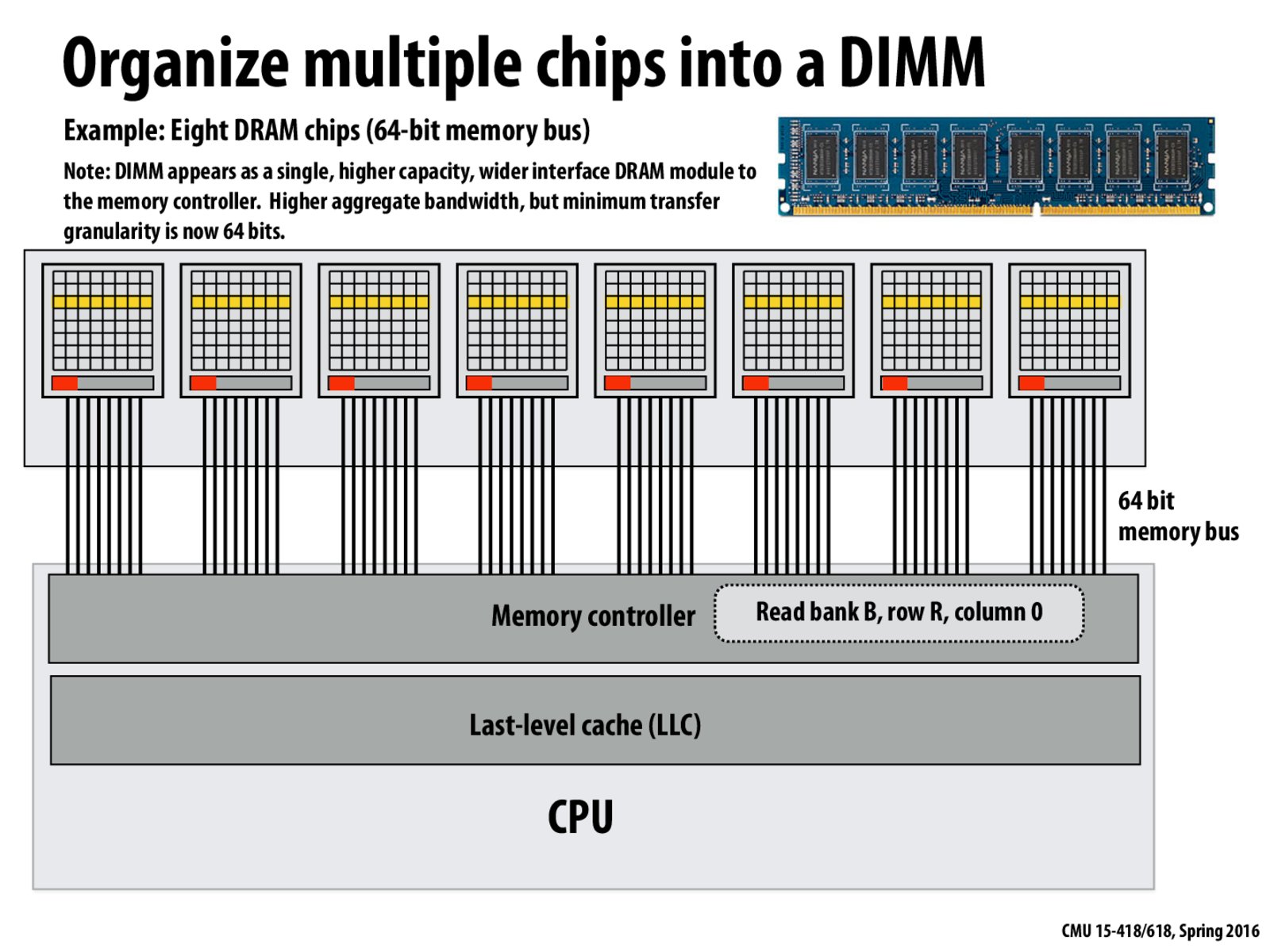
Can someone make an analogy between what's going on in this slide and SIMD?
Now say a processor wanted to load a cache line from memory. Can you think of a really bad way to store this cache line's worth of data on the DIMM such that in order to send this line over the data bus, we would have to execute a sequence of memory load instructions that get very poor utilization of our 8 sets of 8 pins (analogous to poor SIMD vector lane utilization)?
MaxFlowMinCut
In this slide, the memory controller is reading 8 bytes in parallel from 8 logically separate DRAM chips in a DIMM. This is conceptually similar to SIMD, in which a set of ALUs read inputs from a vector of values in parallel over a single clock cycle. One could imagine that the ALUs are the DRAM chips, and are reading values from the memory controller in parallel (which holds the vector).
A simple really bad way to store the cache line would be to store all bytes of the cache line on a single DRAM chip. In doing so, we would only be able to pull a single byte off of the chip each clock cycle. An even worse way to store the cache line would be to store the line on a single DRAM chip, and store each consecutive byte of the line on a different row. In doing so, we would have to go through the entire pre-charge, write-back, row activation, column selection, pin transfer workflow for every single byte.
karima
@MaxFlowMinCut, right! To add, reading memory from DIMM is similar to SIMD because we are executing one instruction, "Read bank B, row R, col C" in parallel across multiple units of data in lockstep.
aeu
One thing that I do not understand is the relation between the memory bus providing 64 bits of data per request and the cache lines being 64 bytes. Is a single cache line retrieved through multiple memory fetches, which get data from multiple DRAM rows?
Renegade
@aeu, yes, I think it has to be retrieved more than one fetch, but it may not be from multiple rows. Since each row buffer contains a number of bytes, total system would have pretty much data buffered after the first fetch.
ArbitorOfTheFountain
First of all, 64 bits (8 bytes) is retrieved via the memory bus with each access. This 64 bits is typically composed of 8 bits per chip, across 8 chips. To fill a cache line of 64 BYTES, we must read 64 bits 8 times. This is very much linked to part 2 in exercise 6.
BensonQiu
Since the DIMM has a 64-bit memory bus, memory should be stored in 64-bit strides to maximize throughput.
For example, when loading 512 bits (64 bytes) for the cache line, the first DRAM chip would have bits 0:7, 64:71, 128:135, 192:199, ...
maxdecmeridius
For this DIMM, each of these DRAM chips has multiple banks, right?
Can someone make an analogy between what's going on in this slide and SIMD?
Now say a processor wanted to load a cache line from memory. Can you think of a really bad way to store this cache line's worth of data on the DIMM such that in order to send this line over the data bus, we would have to execute a sequence of memory load instructions that get very poor utilization of our 8 sets of 8 pins (analogous to poor SIMD vector lane utilization)?
In this slide, the memory controller is reading 8 bytes in parallel from 8 logically separate DRAM chips in a DIMM. This is conceptually similar to SIMD, in which a set of ALUs read inputs from a vector of values in parallel over a single clock cycle. One could imagine that the ALUs are the DRAM chips, and are reading values from the memory controller in parallel (which holds the vector).
A simple really bad way to store the cache line would be to store all bytes of the cache line on a single DRAM chip. In doing so, we would only be able to pull a single byte off of the chip each clock cycle. An even worse way to store the cache line would be to store the line on a single DRAM chip, and store each consecutive byte of the line on a different row. In doing so, we would have to go through the entire pre-charge, write-back, row activation, column selection, pin transfer workflow for every single byte.
@MaxFlowMinCut, right! To add, reading memory from DIMM is similar to SIMD because we are executing one instruction, "Read bank B, row R, col C" in parallel across multiple units of data in lockstep.
One thing that I do not understand is the relation between the memory bus providing 64 bits of data per request and the cache lines being 64 bytes. Is a single cache line retrieved through multiple memory fetches, which get data from multiple DRAM rows?
@aeu, yes, I think it has to be retrieved more than one fetch, but it may not be from multiple rows. Since each row buffer contains a number of bytes, total system would have pretty much data buffered after the first fetch.
First of all, 64 bits (8 bytes) is retrieved via the memory bus with each access. This 64 bits is typically composed of 8 bits per chip, across 8 chips. To fill a cache line of 64 BYTES, we must read 64 bits 8 times. This is very much linked to part 2 in exercise 6.
Since the DIMM has a 64-bit memory bus, memory should be stored in 64-bit strides to maximize throughput.
For example, when loading 512 bits (64 bytes) for the cache line, the first DRAM chip would have bits 0:7, 64:71, 128:135, 192:199, ...
For this DIMM, each of these DRAM chips has multiple banks, right?
@maxdecmeridius: yup