Just to clarify my understanding of what is happening here, does this idea of pipelining multiple memory requests using multiple banks correspond to the idea of hiding stalls using multi-threading, as demonstrated on this slide
temmie
@ote I think it more clearly parallels (:P) the way we discussed pipelining in lecture 7 (for instance, here: http://15418.courses.cs.cmu.edu/spring2016/lecture/progperf2/slide_027), where we're trying to maximize utilization of a resource that causes a slow step in the process, which here would be the data pins and the CAS step. But yes, you could put each thread in a row like the banks are here, with "processing" and "memory fetch" blocks, and we align them so that the "processing" blocks can overlap "memory fetch" (but not each other!) vertically, since the processor is the shared resource we want to fully utilize.
Interestingly, "memory fetch" blocks in different threads can also overlap. So far in the course, we've always considered memory stalls as a constant amount of time regardless of how many memory fetches are happening at once. But as we see a bit in this lecture, we can't actually always serve multiple requests at once, right? Or is the majority of the time taken by the data being transferred, or the signals traveling through the hardware, such that any delay from conflicts between multiple simultaneous requests would have a negligible effect on the total?
xiaoguaz
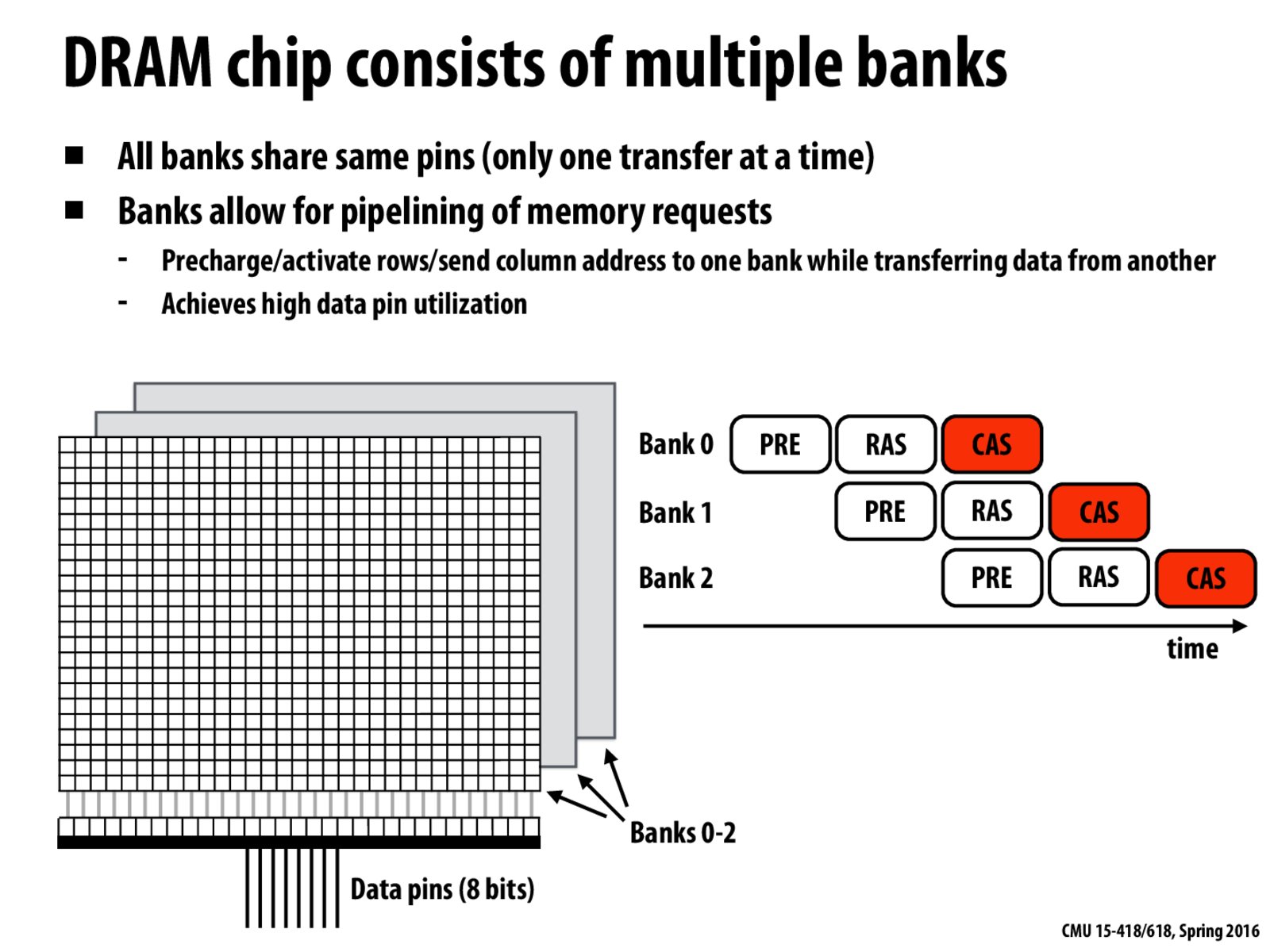
For this method, I think it is to improve the throughput rather than reduce the latency.
However, I have a problem here. I think the PRE step is push data back to the row, RAS step is to copy the row into buffer (not sure), CAS is to send data to pins. So how can these three operations happen at the same time since we only have on buffer?
temmie
@xiaoguaz Well, multithreading hides latency and improves throughput (it doesn't reduce latency for a single thread, and actually often increases it). So all three approaches are intended to improve throughput by "overlapping" work.
On slide 11 you can see that the three steps are associated with different sections of the chip that shouldn't conflict. I think RAS is activation of the row in the bank (not the row buffer), and then everything to do with the buffer and pins is combined into the CAS step.
Araina
From my point of view, it is to improve the throughput by hiding latency.
PRE is to establish a baseline voltage to get banks ready for reading or writing.
RAS is to read a specific row of data into the row buffer.
CAS is to access a particular column in the current row buffer.
Each bank can be precharged by hardware, and each of them has a single row buffer, which can be accessed by data pins separately. Thus these steps can be parallel executed by multiple banks on DRAM.
maxdecmeridius
So just to be clear, each bank has its own row buffer, but there are still only 8 data pins (probably because the row buffer outputs go through a multiplexer before reaching the data pins).
@maxdecmeridius @yangwu I thought there was only one row buffer per set of data pins, but I guess I'm not certain of that... the reference is definitely relevant and has more information, but I don't see where it specifies one buffer per bank in the pipelined case--is there a particular slide you're looking at?
xiaoguaz
@temmie @Araina Thank you for clarifying before. I think if there are only one buffer for multiple banks, there won't be able to parallel the operation of RAS and CAS. If there one buffer for every banks, I can understand why it works.
Araina
As I stated, each DRAM bank has one row buffer.
Just type this sentence in google and one can find many evidences.
yangwu
@temmie I was looking at the picture at slide 3
temmie
Ah, yeah, in the lecture video (about 27 minutes in) Kayvon specifically says they each have their own row buffer. So all the row buffers are connected to the same set of data pins?
Araina
@temmie, yes, there's a single set of data pins (8 bits) here. Basically, the reason why one DRAM chip consists of multiple banks is to fully utilize these data pins.
cmusam
Previously, we mentioned that at most of the clock ticks, the pins are waiting for the other operations (precharge, row activation etc.) to complete. Here, we have multiple arrays connected to the same pins to hide latency.
Just to clarify my understanding of what is happening here, does this idea of pipelining multiple memory requests using multiple banks correspond to the idea of hiding stalls using multi-threading, as demonstrated on this slide
@ote I think it more clearly parallels (:P) the way we discussed pipelining in lecture 7 (for instance, here: http://15418.courses.cs.cmu.edu/spring2016/lecture/progperf2/slide_027), where we're trying to maximize utilization of a resource that causes a slow step in the process, which here would be the data pins and the CAS step. But yes, you could put each thread in a row like the banks are here, with "processing" and "memory fetch" blocks, and we align them so that the "processing" blocks can overlap "memory fetch" (but not each other!) vertically, since the processor is the shared resource we want to fully utilize.
Interestingly, "memory fetch" blocks in different threads can also overlap. So far in the course, we've always considered memory stalls as a constant amount of time regardless of how many memory fetches are happening at once. But as we see a bit in this lecture, we can't actually always serve multiple requests at once, right? Or is the majority of the time taken by the data being transferred, or the signals traveling through the hardware, such that any delay from conflicts between multiple simultaneous requests would have a negligible effect on the total?
For this method, I think it is to improve the throughput rather than reduce the latency.
However, I have a problem here. I think the PRE step is push data back to the row, RAS step is to copy the row into buffer (not sure), CAS is to send data to pins. So how can these three operations happen at the same time since we only have on buffer?
@xiaoguaz Well, multithreading hides latency and improves throughput (it doesn't reduce latency for a single thread, and actually often increases it). So all three approaches are intended to improve throughput by "overlapping" work.
On slide 11 you can see that the three steps are associated with different sections of the chip that shouldn't conflict. I think RAS is activation of the row in the bank (not the row buffer), and then everything to do with the buffer and pins is combined into the CAS step.
From my point of view, it is to improve the throughput by hiding latency.
PRE is to establish a baseline voltage to get banks ready for reading or writing. RAS is to read a specific row of data into the row buffer. CAS is to access a particular column in the current row buffer.
Each bank can be precharged by hardware, and each of them has a single row buffer, which can be accessed by data pins separately. Thus these steps can be parallel executed by multiple banks on DRAM.
So just to be clear, each bank has its own row buffer, but there are still only 8 data pins (probably because the row buffer outputs go through a multiplexer before reaching the data pins).
Is this correct?
@maxdecmeridius, yes, I think you are right
reference
@maxdecmeridius @yangwu I thought there was only one row buffer per set of data pins, but I guess I'm not certain of that... the reference is definitely relevant and has more information, but I don't see where it specifies one buffer per bank in the pipelined case--is there a particular slide you're looking at?
@temmie @Araina Thank you for clarifying before. I think if there are only one buffer for multiple banks, there won't be able to parallel the operation of RAS and CAS. If there one buffer for every banks, I can understand why it works.
As I stated, each DRAM bank has one row buffer. Just type this sentence in google and one can find many evidences.
@temmie I was looking at the picture at slide 3
Ah, yeah, in the lecture video (about 27 minutes in) Kayvon specifically says they each have their own row buffer. So all the row buffers are connected to the same set of data pins?
@temmie, yes, there's a single set of data pins (8 bits) here. Basically, the reason why one DRAM chip consists of multiple banks is to fully utilize these data pins.
Previously, we mentioned that at most of the clock ticks, the pins are waiting for the other operations (precharge, row activation etc.) to complete. Here, we have multiple arrays connected to the same pins to hide latency.