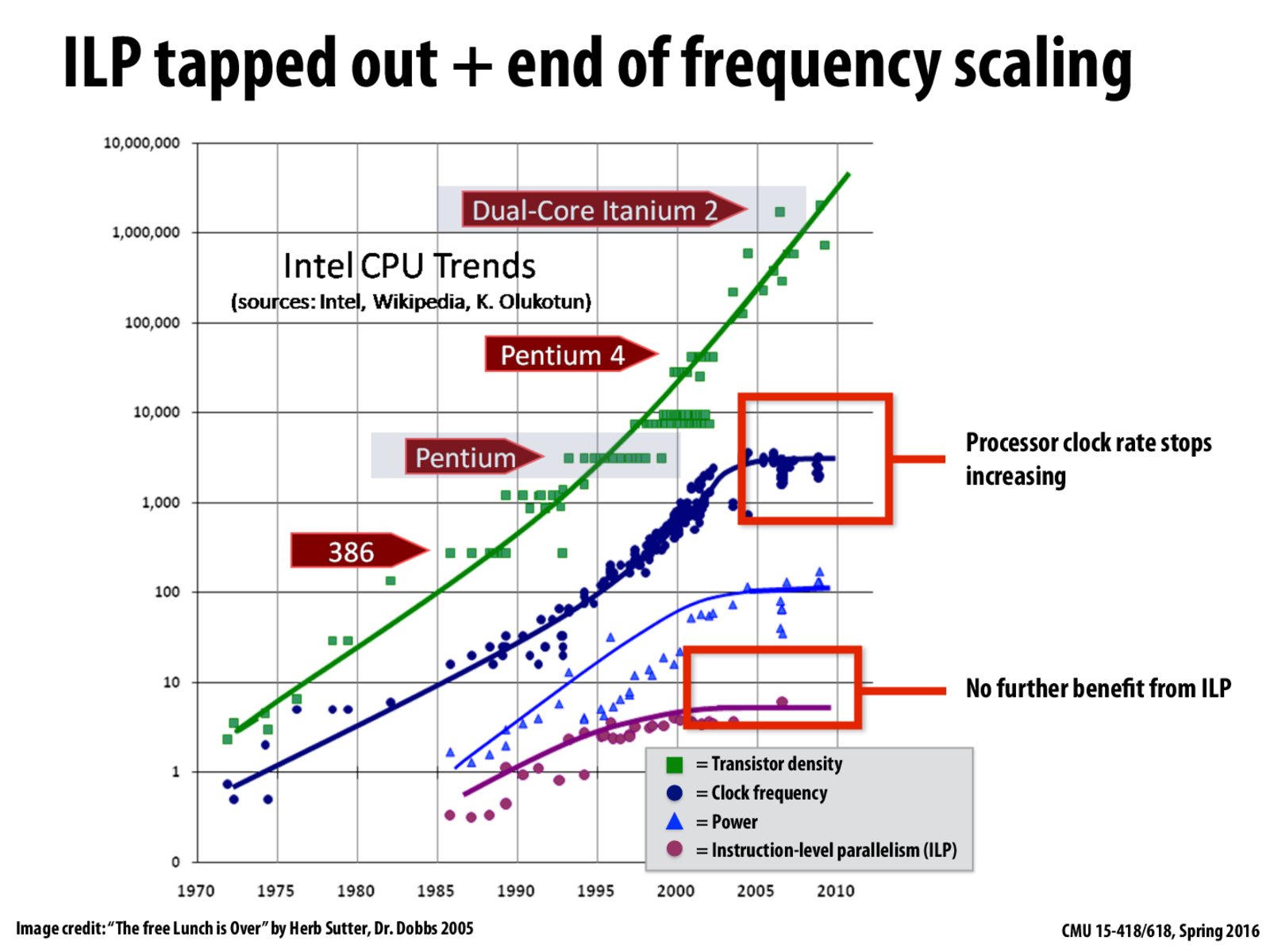
An interesting feature of this graph is that the green line (the number of transistors per unit area) is still going up. Note it's this green line that's most closely related to Moore's Law.
This graph stops at 2010, but it's now 2015 and looking forward a decade or so there's considerable concern about the ability to continue to increase transistor density due to the breakdown of what has been a very convenient property of transistors: that as transistors shrink they use less power.
This property is often referred to as Denard scaling. Dennard scaling tells us that as a transistor shrinks, so does its required operating voltage and current. The result is that each transistor requires less power and, as a result, the power density of transistors (power consumed per unit area of chip real estate) stays roughly constant as technology improves and transistors shrink. In other words, Dennard scaling says that if today you have a chip with T transistors, and in the future you can pack 2T transistors into a chip with the same area, that new chip will still consume roughly the same amount as power as the current one. (This is a good thing. In a multi-core world, that means you could have two cores in the future for the energy cost of one core today.)
The "breakdown of Dennard scaling" is referring to the fact that we're quickly approaching a realm where we can no longer reduce transistor power consumption proportionally with its size (one example is that voltages are now nearing threshold voltages, the minimum voltages required to operate the transistor.) As a result, the power density may begin to go up.
So even though technology development is still proceeding in a manner that we can cram more and more transistors onto a chip of fixed size, in the future we'll reach a point were can't use them all at the same time because using them will require too much power. You'll hear a controversial term thrown around these days called "Dark Silicon", referring to the fact that future chips may not be able to use all their transistors at the same time.
I'm confused about the blue line with triangles that graphs power. It seems that the amount of transistors increases exponentially after 2005, and the amount of power stays roughly the same. So the amount of power per transistor is decreasing in that part of the graph.
But why was there an increase in power as transistor size decreased from around 1985-2000? This seems to contradict Dennard scaling.
kayvonf
@dhua. Notice the increase in power tracks frequency. Dennard scaling tells us that power-per transistor, that is... power density (power per unit chip area) stays the same -- iso-frequency.
patrickbot
Why does the clock rate line grows sharply around 2000? Is it because we couldn't see more improvements from ILP, so more work was put into improving clock rate?
Lawliet
In this graph, we observe Moore's law all the way up to 2010. However, we start seeing the diminishing returns on Clock frequency, and ILP to save up on power usage all the way back around 2003-2004. From 2004-2010, transistor density still seems to go strong in its exponential increase. What is the reason for the continued interest in increasing transistor density at this point? My guess is that the chips are getting smaller, but is there another benefit or reason that we would be interested in aggressively pursuing a more transistor dense chip?
edit: I was reading the instructor note and was wondering if another benefit of pursuing transistor density was also to use less power due to the property that "as transistors shrink they use less power"
hofstee
@Lawliet: Transistor density increasing means we can cram more "stuff" on the die as well. We can add larger (but faster) adders, FPUs, or other things. Recently, Intel has been using more and more of their die space to add a pretty decent integrated GPU, but there are loads of other improvements that most people don't immediately think about such as improved branch predictors, and larger caches. Other things could include improved interconnects between the CPU cores, larger and more varied I/O and memory controllers, registers, and more.
It also reduces the cost to make a chip (smaller transistors means more chips per wafer, even if the cost to make one wafer is larger there are usually enough chips per wafer to make it worthwhile).
haibinl
For your interest, the author of this figure wrote another article Welcome to the Jungle on the trend of mainstream hardware after 2005. In this article, he talked about the trend to produce multicore, heterogeneous cores and elastic compute cloud cores, as well as the implication for programmers nowadays. It's not as technical as the one provided by Professor Kayvon but quite readable.
aeu
How does the recent trend of die size shrinkage translate to this scale? I have heard that as the dies sizes shrink, the electromagnetic interference between transistors start becoming a significant problem. Would that mean that after some point of fitting more and more transistors into a die of specific size, the amount we can fit won't increase and we would need to increase the physical areas of dies (for example, going from a standard-size consumer-grade Intel processor to a CPU board attached to the motherboard) to cram in more cores?
hofstee
@aeu Chipmakers have actually been increasing die size, even though transistor size is decreasing. We probably won't see a huge increase in die size though. The reasons why dies are square-ish is because it best fits a circle, and any errors are usually isolated on one chip. 5nm is about as small as we can go last I heard, and 7nm chips are slated to go into production by 2017.
Increasing die size means an error on making the wafer is much more costly, we can't have 1 die per wafer because you will never* get a usable chip.
To clarify a bit further, Intel follows a "Tick-Tock" pattern with its releases (about every 18 months), the Tick is a shrinking of the process, from 22nm to 14nm for example, and die size usually shrinks. On the Tock, they release a new microarchitecture on the same process size, so die size increases a bit.
Intel recently acquired Altera (an FPGA company) so it might be the case that multiple processors per motherboard or heterogeneous systems are the way forward, unless we can find another manufacturing breakthrough. For those unfamiliar, an FPGA (Field-Programmable Gate Array) is essentially a programmable piece of hardware.
I completely forgot to mention this earlier but I'm editing my comment to add that 3D lithography and other 3D Integrated Circuits are also points of heavy research right now. We can't go smaller, or sideways, so we go up.
maxdecmeridius
If industry was going to raise the power thresholds, and in general allow chips to consume more energy, would we be able to continue Moore's law (for a couple more years at least)?
dhua
@maxdecmerididus
I think the problem with increasing power is that the heat resulting from using more power would melt the chip. Unless a new chip material and/or cooling method is discovered, I don't think raising power thresholds would help.
How Moore's law will continue depends on what new technology is discovered in the future, rather than limitations of current existing technology. The assumption that we will still be using the same type of transistors in the future might not be true.
traveling_saleswoman
It seems like currently research being done on the most effective ways to utilize the transistors that can be fit onto a chip. @hofstee's answer mentions 3D integrated circuits, which I understand to be circuits with more transistors available but which use less additional power than simply adding transistors to a 2D chip. However, has there been research in materials science or ECE investigating more efficient cooling methods for the chip, or is the "power wall" unmovable?
One thing that come to mind as a way to cool processors down is using wires with lower resistance. Superconducting wires would heat up less, pushing the power wall off little later. However it seems that superconductors only emerge at extremely low temperatures, so they couldn't be used in everyday computing. Does anyone know more about this area?
For those interested:
An interesting feature of this graph is that the green line (the number of transistors per unit area) is still going up. Note it's this green line that's most closely related to Moore's Law.
This graph stops at 2010, but it's now 2015 and looking forward a decade or so there's considerable concern about the ability to continue to increase transistor density due to the breakdown of what has been a very convenient property of transistors: that as transistors shrink they use less power.
This property is often referred to as Denard scaling. Dennard scaling tells us that as a transistor shrinks, so does its required operating voltage and current. The result is that each transistor requires less power and, as a result, the power density of transistors (power consumed per unit area of chip real estate) stays roughly constant as technology improves and transistors shrink. In other words, Dennard scaling says that if today you have a chip with
Ttransistors, and in the future you can pack2Ttransistors into a chip with the same area, that new chip will still consume roughly the same amount as power as the current one. (This is a good thing. In a multi-core world, that means you could have two cores in the future for the energy cost of one core today.)The "breakdown of Dennard scaling" is referring to the fact that we're quickly approaching a realm where we can no longer reduce transistor power consumption proportionally with its size (one example is that voltages are now nearing threshold voltages, the minimum voltages required to operate the transistor.) As a result, the power density may begin to go up.
So even though technology development is still proceeding in a manner that we can cram more and more transistors onto a chip of fixed size, in the future we'll reach a point were can't use them all at the same time because using them will require too much power. You'll hear a controversial term thrown around these days called "Dark Silicon", referring to the fact that future chips may not be able to use all their transistors at the same time.
The issue is addressed in this article: Power Challenges May End the Multicore Era.
Also, some of you may be interested in Stanford's CPU DB Project, which is the subject of this ACM Queue article: CPU DB: Recording Microprocessor History.
I'm confused about the blue line with triangles that graphs power. It seems that the amount of transistors increases exponentially after 2005, and the amount of power stays roughly the same. So the amount of power per transistor is decreasing in that part of the graph.
But why was there an increase in power as transistor size decreased from around 1985-2000? This seems to contradict Dennard scaling.
@dhua. Notice the increase in power tracks frequency. Dennard scaling tells us that power-per transistor, that is... power density (power per unit chip area) stays the same -- iso-frequency.
Why does the clock rate line grows sharply around 2000? Is it because we couldn't see more improvements from ILP, so more work was put into improving clock rate?
In this graph, we observe Moore's law all the way up to 2010. However, we start seeing the diminishing returns on Clock frequency, and ILP to save up on power usage all the way back around 2003-2004. From 2004-2010, transistor density still seems to go strong in its exponential increase. What is the reason for the continued interest in increasing transistor density at this point? My guess is that the chips are getting smaller, but is there another benefit or reason that we would be interested in aggressively pursuing a more transistor dense chip?
edit: I was reading the instructor note and was wondering if another benefit of pursuing transistor density was also to use less power due to the property that "as transistors shrink they use less power"
@Lawliet: Transistor density increasing means we can cram more "stuff" on the die as well. We can add larger (but faster) adders, FPUs, or other things. Recently, Intel has been using more and more of their die space to add a pretty decent integrated GPU, but there are loads of other improvements that most people don't immediately think about such as improved branch predictors, and larger caches. Other things could include improved interconnects between the CPU cores, larger and more varied I/O and memory controllers, registers, and more.
It also reduces the cost to make a chip (smaller transistors means more chips per wafer, even if the cost to make one wafer is larger there are usually enough chips per wafer to make it worthwhile).
For your interest, the author of this figure wrote another article Welcome to the Jungle on the trend of mainstream hardware after 2005. In this article, he talked about the trend to produce multicore, heterogeneous cores and elastic compute cloud cores, as well as the implication for programmers nowadays. It's not as technical as the one provided by Professor Kayvon but quite readable.
How does the recent trend of die size shrinkage translate to this scale? I have heard that as the dies sizes shrink, the electromagnetic interference between transistors start becoming a significant problem. Would that mean that after some point of fitting more and more transistors into a die of specific size, the amount we can fit won't increase and we would need to increase the physical areas of dies (for example, going from a standard-size consumer-grade Intel processor to a CPU board attached to the motherboard) to cram in more cores?
@aeu Chipmakers have actually been increasing die size, even though transistor size is decreasing. We probably won't see a huge increase in die size though. The reasons why dies are square-ish is because it best fits a circle, and any errors are usually isolated on one chip. 5nm is about as small as we can go last I heard, and 7nm chips are slated to go into production by 2017.
Increasing die size means an error on making the wafer is much more costly, we can't have 1 die per wafer because you will never* get a usable chip.
There's a great quora post about this here.
To clarify a bit further, Intel follows a "Tick-Tock" pattern with its releases (about every 18 months), the Tick is a shrinking of the process, from 22nm to 14nm for example, and die size usually shrinks. On the Tock, they release a new microarchitecture on the same process size, so die size increases a bit.
Intel recently acquired Altera (an FPGA company) so it might be the case that multiple processors per motherboard or heterogeneous systems are the way forward, unless we can find another manufacturing breakthrough. For those unfamiliar, an FPGA (Field-Programmable Gate Array) is essentially a programmable piece of hardware.
I completely forgot to mention this earlier but I'm editing my comment to add that 3D lithography and other 3D Integrated Circuits are also points of heavy research right now. We can't go smaller, or sideways, so we go up.
If industry was going to raise the power thresholds, and in general allow chips to consume more energy, would we be able to continue Moore's law (for a couple more years at least)?
@maxdecmerididus
I think the problem with increasing power is that the heat resulting from using more power would melt the chip. Unless a new chip material and/or cooling method is discovered, I don't think raising power thresholds would help.
How Moore's law will continue depends on what new technology is discovered in the future, rather than limitations of current existing technology. The assumption that we will still be using the same type of transistors in the future might not be true.
It seems like currently research being done on the most effective ways to utilize the transistors that can be fit onto a chip. @hofstee's answer mentions 3D integrated circuits, which I understand to be circuits with more transistors available but which use less additional power than simply adding transistors to a 2D chip. However, has there been research in materials science or ECE investigating more efficient cooling methods for the chip, or is the "power wall" unmovable?
One thing that come to mind as a way to cool processors down is using wires with lower resistance. Superconducting wires would heat up less, pushing the power wall off little later. However it seems that superconductors only emerge at extremely low temperatures, so they couldn't be used in everyday computing. Does anyone know more about this area?