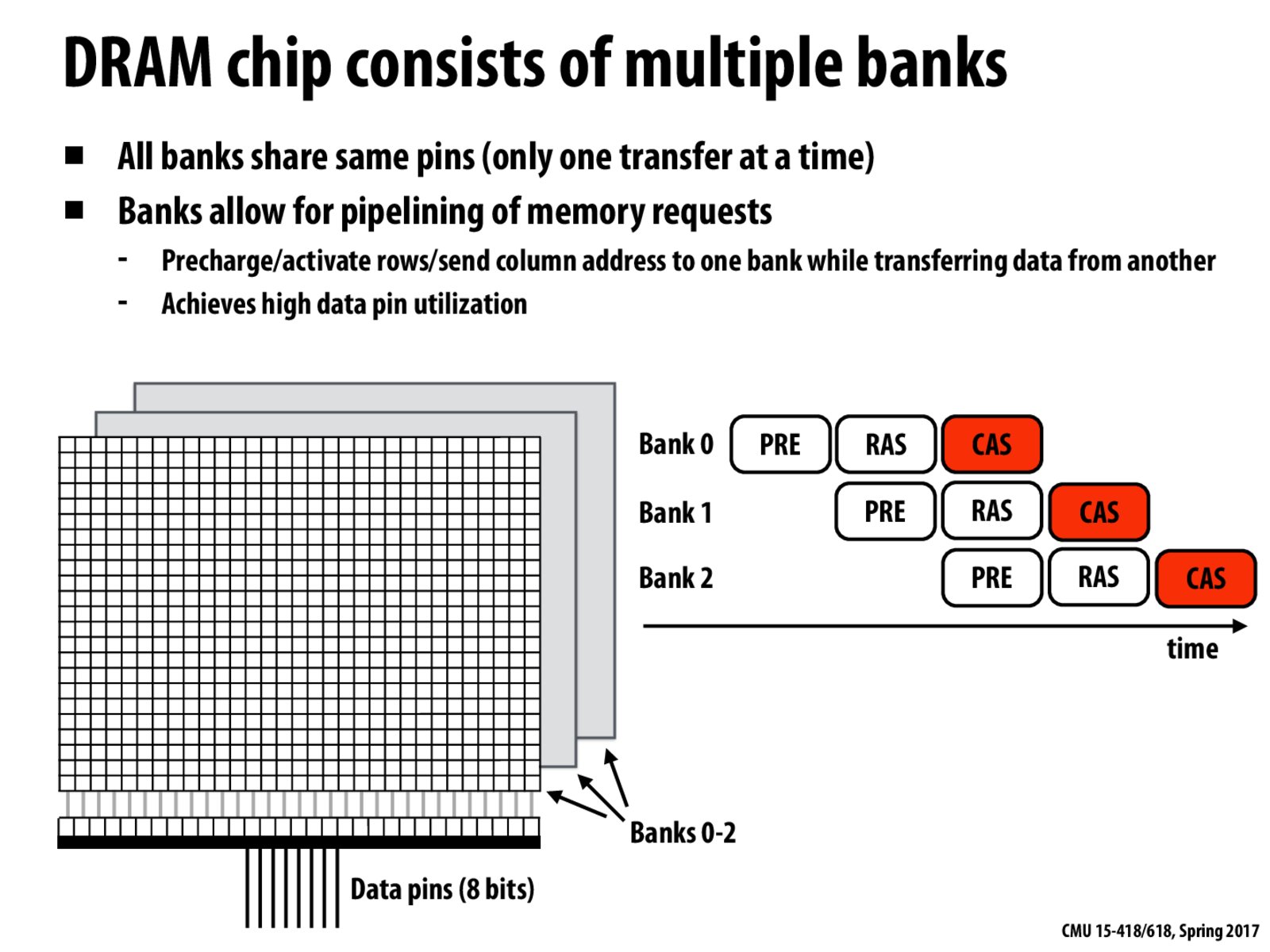
This particular arrangement allows for 100% utilization of the data pins.
chenh1
What is the difference between pipeline and interleaving in banks? Can we use both techniques simultaneously?
cwchang
Pipelining through multiple banks are similar to multiple executors for processing instructions. They can effectively hide the latency but not reduce them.
bochet
If so, why should there be more than 3 banks in modern DRAM?
paramecinm
@bochet If we read consecutive bytes in one bank, there will be more CAS parts in the pipeline and can hide more banks' latency.
pk267
These banks hold interleaved addresses, and not contiguous memory addresses. See here - https://en.wikipedia.org/wiki/Interleaved_memory to see why.
crabcake
Is row buffer a part of data pins?
planteurJMTLG
@crabcake No, according to this website, "Each DRAM bank has one row-buffer".
life
both bank interleaving and channel interleaving (as is discussed in next slide) are interleaved memory design
sherwood
Does each bank hold a separate copy of the entire memory?
Cake
No, as I understand it each bank holds different memory.
srb
Agree - each bank holds different memory.
mak
To achieve 100% pin utilization for this 3 bank arrangement, don't we need to assume that PRE, RAS and CAS, all these three phases take equal time? If that's not true and PRE/RAS take more time than CAS, don't we need either more banks or more CAS(e.g. in burst mode)?
sushi
@mak, I think it will need (PRE+RAS)/CAS bands to hide the latency of row activation process and fully use the pin. Therefore, increasing band count or having larger CAS both work here.
This particular arrangement allows for 100% utilization of the data pins.
What is the difference between pipeline and interleaving in banks? Can we use both techniques simultaneously?
Pipelining through multiple banks are similar to multiple executors for processing instructions. They can effectively hide the latency but not reduce them.
If so, why should there be more than 3 banks in modern DRAM?
@bochet If we read consecutive bytes in one bank, there will be more CAS parts in the pipeline and can hide more banks' latency.
These banks hold interleaved addresses, and not contiguous memory addresses. See here - https://en.wikipedia.org/wiki/Interleaved_memory to see why.
Is row buffer a part of data pins?
@crabcake No, according to this website, "Each DRAM bank has one row-buffer".
both bank interleaving and channel interleaving (as is discussed in next slide) are interleaved memory design
Does each bank hold a separate copy of the entire memory?
No, as I understand it each bank holds different memory.
Agree - each bank holds different memory.
To achieve 100% pin utilization for this 3 bank arrangement, don't we need to assume that PRE, RAS and CAS, all these three phases take equal time? If that's not true and PRE/RAS take more time than CAS, don't we need either more banks or more CAS(e.g. in burst mode)?
@mak, I think it will need (PRE+RAS)/CAS bands to hide the latency of row activation process and fully use the pin. Therefore, increasing band count or having larger CAS both work here.