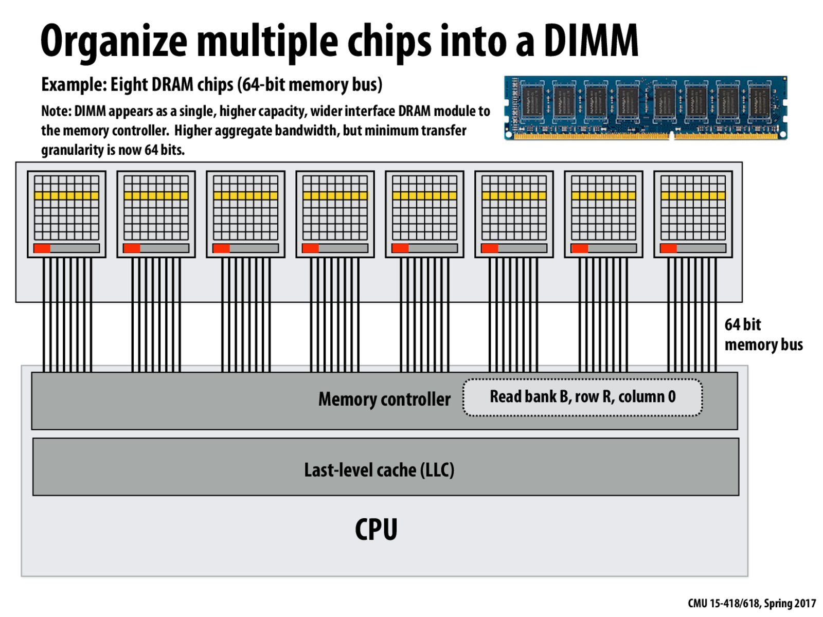
On the chip pictured, Kayvon noted that there are 8 DIMMs, and asked what the 9th would be if there were one more. To this, someone responded "ECC"
ECC, or "Error-correcting code memory," can be used to detect and possibly correct errors in the other 8 DIMMs. Think parity bit checks, or Hamming codes.
For those familiar with hardware, bit errors are not to be ignored. They can occur because of hardware failure, or if your computer is being used in a non-ideal environment (e.g. in a nuclear power plant, the ISS).
chenh1
The memory controller will be responsible for constructing the most effective sequence of memory operations and send requests to DRAM.
A DIMM is a collection of multiple DRAM chips each with its own data pins and then each chip has multiple banks. But the banks share the chip's data pins.
kapalani
Just to confirm, each of the 8 boxes here represents a DRAM chip and within each of these boxes, we have several banks? If this is the case I have 2 questions:
Why doesn't the memory controller specify which chip to read from. Isn't that information needed/correspond to some bits of the physical address?
Don't the layouts for consecutive addresses between this slide and the previous slide kind of conflict since we want to lay out consecutive addresses across different banks in a chip to allow for pipelining accesses to consecutive addresses and with multiple channels we want to lay out consecutive addresses across the different chips? Or is consecutive addresses refer to different strides in these 2 cases?
hzxa21
A DIMM to memory is like a core to CPU, and a bank within each DIMM is like execution context within each core.
atadkase
@kapalani
Generally when a cache miss occurs, the entire cache line is fetched as opposed to fetching a single byte. In this case, the cache line is spread across chips, and that's why you don't need to specify a single chip. You end up reading all the chips.
This might help you to think about it, but in reality the DRAM controller might decide to scramble the locations.
Cache lines (0 -n) -> One row of Memory Bank 0 of all chips.
Cache lines (n+1 - 2n+1) -> One row of Memory Bank 1 of all chips, and so on.
MichaelJordan
You read all the chips at the same time, which is great because then you get 64 bytes simultaneously rather than just 8. This fully utilizes the 64 byte wide memory bus.
On the chip pictured, Kayvon noted that there are 8 DIMMs, and asked what the 9th would be if there were one more. To this, someone responded "ECC"
ECC, or "Error-correcting code memory," can be used to detect and possibly correct errors in the other 8 DIMMs. Think parity bit checks, or Hamming codes.
For those familiar with hardware, bit errors are not to be ignored. They can occur because of hardware failure, or if your computer is being used in a non-ideal environment (e.g. in a nuclear power plant, the ISS).
The memory controller will be responsible for constructing the most effective sequence of memory operations and send requests to DRAM.
DIMM - dual in-line memory module
A DIMM is a collection of multiple DRAM chips each with its own data pins and then each chip has multiple banks. But the banks share the chip's data pins.
Just to confirm, each of the 8 boxes here represents a DRAM chip and within each of these boxes, we have several banks? If this is the case I have 2 questions:
Why doesn't the memory controller specify which chip to read from. Isn't that information needed/correspond to some bits of the physical address?
Don't the layouts for consecutive addresses between this slide and the previous slide kind of conflict since we want to lay out consecutive addresses across different banks in a chip to allow for pipelining accesses to consecutive addresses and with multiple channels we want to lay out consecutive addresses across the different chips? Or is consecutive addresses refer to different strides in these 2 cases?
A DIMM to memory is like a core to CPU, and a bank within each DIMM is like execution context within each core.
@kapalani
Generally when a cache miss occurs, the entire cache line is fetched as opposed to fetching a single byte. In this case, the cache line is spread across chips, and that's why you don't need to specify a single chip. You end up reading all the chips.
This might help you to think about it, but in reality the DRAM controller might decide to scramble the locations. Cache lines (0 -n) -> One row of Memory Bank 0 of all chips. Cache lines (n+1 - 2n+1) -> One row of Memory Bank 1 of all chips, and so on.
You read all the chips at the same time, which is great because then you get 64 bytes simultaneously rather than just 8. This fully utilizes the 64 byte wide memory bus.