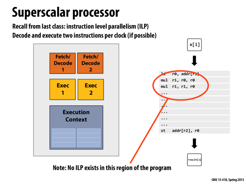
Question: Why are there two orange boxes in this diagram, and how useful is this setup given the example program circled above?
lament
In this case, we are contrasting single core performance with multi-core performance. In particular, multiple cores only help when you can "split-up" a task. Here, the first three instruction lines listed are "linearly" dependent on each other, and thus we cannot run the lines separately or out of order. In this case, then, we would have been better off with one powerful core as opposed to two weaker cores.
Actually, I want to check myself here: which parts of the CPU are we referring to as "the core" generically? Is it proper to refer to the above as "multiple cores"? I could probably find the answer in the next few slides, but I'll let my fellow students stab at it.
BigFish
@lament In my understanding, in this picture we only have one core. There are two fetch/decode units and two execution units in the core. So we have the potentiality to execute two instructions at the same time.
However, in this case, since the instructions in the circle are not independent, we can only execute one instruction one time.
kayvonf
@lament: Terminology is incredibly lose in the field with respect to what is a processor? what is a core? etc. Intel and most traditional CPU companies use the notion of a core that I've adopted in this lecture. I consider a core to be a largely-self contained unit on the chip that is capable of executing an instruction stream (it contains fetch/decode capability, execution capability, and storage for thread contexts). Under this reasoning, the illustration above depicts one core.
A multi-core processor is a processor that has several replications of this basic block. A quad-core processor, such as the Intel chip on slide_021 has this basic block replicated four times. Of course, certain components of a chip might be shared across cores. For example, in the quad-core Intel chip I lined to above, there is an L3 that is shared among the cores (each of the cores has their own L1 and L2).
However, I should caution you that forcing yourself to write down a precise definition of what a "core" is might cause you a lot of frustration, particularly when we start talking about GPUs. What's important is to develop a notion of what the basic components (fetch/decode, execution units, execution contexts) do, and understand the key design principles that are intended run programs with independent work (work that can potentially be run in parallel) more efficiently...
kayvonf
As a follow up: The particular way architecture is explained in this lecture has roots way back in 2008 when many experts in the industry were struggling with how to define a core and talk about all these new parallel chips.
"In contrast to ATI and Nvidia, Intel would seem to be at a significant disadvantage in the number of cores it is offering. Next-generation ATI and Nvidia chips will have 800 and 256 cores respectively, said Jon Peddie, president of Jon Peddie Research in Tiburon, Calif."
Here's a blog post I wrote back at the time, when I was frustrated about the lack of consistent terminology (and the confusion in the Times article):
So, I'm a bit confused about some distinctions between superscalar and SIMD. Someone tell me if I'm right: Superscalar execution is automatically done by the hardware when it finds independent instructions. This involves simultaneously running the independent instructions on different ALUs. SIMD however, involves broadcasting the same instruction to all ALUs in the core, the only difference being that these instructions work on different data in each ALU.
So superscalar demonstrates that different commands can run simultaneously, and SIMD demonstrates that the programmer can have some manual control over parallelizing instructions among ALUs.
If this is the case, what's to stop a programmer from manually making use of multiple ALUs to run non-identical instructions simultaneously? Is there a concept of this? How reasonable/possible/useful is it?
kayvonf
@sgbowen: I think you've got it. However, I'm not sure what you mean by "superscalar demonstrates that different commands can run simultaneously" Superscalar execution finds instructions to run simultaneously from a basic sequential instruction stream.
With respect to your comment: If this is the case, what's to stop a programmer from manually making use of multiple ALUs to run non-identical instructions simultaneously? Is there a concept of this? How reasonable/possible/useful is it?
The answer is yes!. A VLIW architecture is an example of an ISA design that gives the programmer (or a compiler) that level of control. The philosophy of a VLIW system is: why burn chip resources (transistors, power, design time, etc.) trying to figure out what instructions can be executed in parallel, when this can all be figured out statically by a compiler, or by a low-level programmer?
Well, it turns out that there's some good reasons to have the chip figure this out, and have it figure it out dynamically.
There's more information around at runtime to know when data dependencies actually exist. (e.g., memory addresses are known, etc.)
The chip designer is the only party that's going to know the hairy details of the internals of a chip, so it's scheduling decisions, unlike a compiler's, can be performed with those details in mind.
If the parallelization/mapping decision is made statically, the program must be recompiled to run well on a new architecture with different numbers of execution resources or different performance characteristics. This is non-starter for a lot of applications in the world.
sgbowen
@kayvonf Thanks, that makes sense!
By that quote, I just meant that the existence of superscalar execution implies that ALUs can handle non-identical instructions (in this case from the same sequential stream) simultaneously, whereas they handle identical instructions when used by SIMD.
sam
This picture seems little confusing to me. A super-scalar processor works on single instruction stream but can process instructions out of order because of presence of multiple execution units. In this diagram it shows 2 fetch and decode units which infers that there can be 2 simultaneous instruction streams that can be processed. It should be a 2-wide single fetch and decode unit which can have single in-order instruction stream as input.
kayvonf
@sam: interpret the two fetch and decode units as functionality to fetch and decode two instructions. The single instruction stream comes from the fact that there's only one execution context for the chip (and hence only once set of registers, etc.)
Notice that the Pentium 4 block diagram on slide 12 has three decode units (see orange box) indicating the ability to decode up to three instructions in a clock (3-way superscalar).
sanchuah
@vrkrishn:these two orange boxes mean it is possible to fetch two instructions and execute them simultaneously from a stream.
Question: Why are there two orange boxes in this diagram, and how useful is this setup given the example program circled above?
In this case, we are contrasting single core performance with multi-core performance. In particular, multiple cores only help when you can "split-up" a task. Here, the first three instruction lines listed are "linearly" dependent on each other, and thus we cannot run the lines separately or out of order. In this case, then, we would have been better off with one powerful core as opposed to two weaker cores.
Actually, I want to check myself here: which parts of the CPU are we referring to as "the core" generically? Is it proper to refer to the above as "multiple cores"? I could probably find the answer in the next few slides, but I'll let my fellow students stab at it.
@lament In my understanding, in this picture we only have one core. There are two fetch/decode units and two execution units in the core. So we have the potentiality to execute two instructions at the same time.
However, in this case, since the instructions in the circle are not independent, we can only execute one instruction one time.
@lament: Terminology is incredibly lose in the field with respect to what is a processor? what is a core? etc. Intel and most traditional CPU companies use the notion of a core that I've adopted in this lecture. I consider a core to be a largely-self contained unit on the chip that is capable of executing an instruction stream (it contains fetch/decode capability, execution capability, and storage for thread contexts). Under this reasoning, the illustration above depicts one core.
A multi-core processor is a processor that has several replications of this basic block. A quad-core processor, such as the Intel chip on slide_021 has this basic block replicated four times. Of course, certain components of a chip might be shared across cores. For example, in the quad-core Intel chip I lined to above, there is an L3 that is shared among the cores (each of the cores has their own L1 and L2).
However, I should caution you that forcing yourself to write down a precise definition of what a "core" is might cause you a lot of frustration, particularly when we start talking about GPUs. What's important is to develop a notion of what the basic components (fetch/decode, execution units, execution contexts) do, and understand the key design principles that are intended run programs with independent work (work that can potentially be run in parallel) more efficiently...
As a follow up: The particular way architecture is explained in this lecture has roots way back in 2008 when many experts in the industry were struggling with how to define a core and talk about all these new parallel chips.
It was even confusing the New York Times and Mr. Jon Peddie. http://www.nytimes.com/2008/08/04/technology/04intel.html
Quoted:
"In contrast to ATI and Nvidia, Intel would seem to be at a significant disadvantage in the number of cores it is offering. Next-generation ATI and Nvidia chips will have 800 and 256 cores respectively, said Jon Peddie, president of Jon Peddie Research in Tiburon, Calif."
Here's a blog post I wrote back at the time, when I was frustrated about the lack of consistent terminology (and the confusion in the Times article):
How to Count to 800 (comparing the NV GTX 280, ATI Radeon 4870, and what I hear about Intel's Larrabee
So, I'm a bit confused about some distinctions between superscalar and SIMD. Someone tell me if I'm right: Superscalar execution is automatically done by the hardware when it finds independent instructions. This involves simultaneously running the independent instructions on different ALUs. SIMD however, involves broadcasting the same instruction to all ALUs in the core, the only difference being that these instructions work on different data in each ALU.
So superscalar demonstrates that different commands can run simultaneously, and SIMD demonstrates that the programmer can have some manual control over parallelizing instructions among ALUs.
If this is the case, what's to stop a programmer from manually making use of multiple ALUs to run non-identical instructions simultaneously? Is there a concept of this? How reasonable/possible/useful is it?
@sgbowen: I think you've got it. However, I'm not sure what you mean by "superscalar demonstrates that different commands can run simultaneously" Superscalar execution finds instructions to run simultaneously from a basic sequential instruction stream.
With respect to your comment: If this is the case, what's to stop a programmer from manually making use of multiple ALUs to run non-identical instructions simultaneously? Is there a concept of this? How reasonable/possible/useful is it?
The answer is yes!. A VLIW architecture is an example of an ISA design that gives the programmer (or a compiler) that level of control. The philosophy of a VLIW system is: why burn chip resources (transistors, power, design time, etc.) trying to figure out what instructions can be executed in parallel, when this can all be figured out statically by a compiler, or by a low-level programmer?
Well, it turns out that there's some good reasons to have the chip figure this out, and have it figure it out dynamically.
@kayvonf Thanks, that makes sense!
By that quote, I just meant that the existence of superscalar execution implies that ALUs can handle non-identical instructions (in this case from the same sequential stream) simultaneously, whereas they handle identical instructions when used by SIMD.
This picture seems little confusing to me. A super-scalar processor works on single instruction stream but can process instructions out of order because of presence of multiple execution units. In this diagram it shows 2 fetch and decode units which infers that there can be 2 simultaneous instruction streams that can be processed. It should be a 2-wide single fetch and decode unit which can have single in-order instruction stream as input.
@sam: interpret the two fetch and decode units as functionality to fetch and decode two instructions. The single instruction stream comes from the fact that there's only one execution context for the chip (and hence only once set of registers, etc.)
Notice that the Pentium 4 block diagram on slide 12 has three decode units (see orange box) indicating the ability to decode up to three instructions in a clock (3-way superscalar).
@vrkrishn:these two orange boxes mean it is possible to fetch two instructions and execute them simultaneously from a stream.