I think I can do a better job of explaining the geometry of the memory system than I did in today in class, so I'll summarize slides 7-14 again here.
A DRAM is 2D array of cells, where a capacitor per cell holds a charge, indicating whether the corresponding bit's value is 1 or 0.
Bitlines (vertical lines) read charge from cells in the selected row from the DRAM array.
Activation: is the act of reading the charge from a selected row into the row buffer. An analog-to-digital converter converts charge on bit-lines to digital values stored in the row buffer. We often say the row whose contents are stored in the row buffer is the "open" row.
Precharge: Reading charge from the capacitors discharges them, destroying the information in each cell. The information must be but back into the DRAM array after an activation, otherwise information is lost! Precharge is the process of "closing" the currently active row and readying the DRAM to read data from a new row. It involves transferring the contents of the row buffer back into the active row's capacitors and resets the bit-lines.
Data from the row buffer is transferred from the DRAM to the processing over the memory bus. In these slides the bus connected to the DRAM is 8-bits wide. That is, it transfers 8 bits of information per clock.
We talked about activation and precharge are overheads of "opening" a new row. These overheads mean that although the DRAM is physically capable of transferring 8 bits per clock, the DRAM can't supply it with information at this rate (e.g., since its busy performing a precharge). This is bad, since the memory bus is one of the scarcest resources in the system. We want to keep it busy as much as possible.
A single DRAM chip will contain multiple DRAM arrays, often called DRAM banks to enable pipelined interleaved processing of memory comments. While one bank is busy handling activation or precharge step, another bank can be actively transferring information over the bus. This idea of interleaving to maintain peak utilization of a shared resource should be very familiar to you!
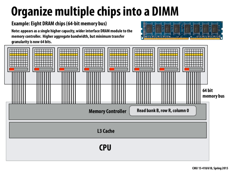
Techniques like DRAM banking and burst transfer modes help the chip realize peak chip bandwidth: 8 bits per clock. To achieve higher bandwidth we simply need a wider bus. Architects achieve this by placing eight DRAM chips together on a DIMM. A single memory command sent to a DIMM results in responses by all eight chips over 8 parallel busses, which is effectively a 64-bit bus to the DIMM (this bus logically constitutes a DRAM channel) Each memory channel supplies 64 bits per clock. Also, the minimum granularity of memory transfer is now 64 bits (up from 8 in the single chip scenario).
Further performance can be achieved by adding additional memory channels. Each channel operates independently, receiving different memory commands, using a physically unique bus.
Note that if you look at the specs of a modern processor, like the Xeon CPUs in latedays, you'll see that the CPU's memory controller supports up to 4 memory channels. This means that to achieve peak memory bandwidth of the system, your computer should have a different DIMM hooked up to each channel. This is why you often must buy DIMMs in groups of 4 these days.
I'm a bit confused. Just to make sure, can the following points be verified if they are correct or not?
In this picture above, we have 8 DRAM chips, each of which have their own DRAM banks.
These 8 chips work as a contiguous block with the address of first cell of the first row of the first chip is 0 and the last cell of the first row of the last chip is (8 * (DRAM array width) -1).
The way we would want to access Bank B, Row R, Col C is roughly -
access Bank B for each DRAM chip and get access (8 * DRAM array width * R) + C
solovoy
So, with 4 channels of DIMM, is the minimum granularity of memory transfer going up from 64 bits to 256 bits or remaining 64 bits (in another word, whether channels are independent)? Also, is this granularity level related to the decision of the cache line size?
kayvonf
@abist: Yes, there are 8 DRAM chips, and to keep things simple I'm illustrating only one bank per chip. DRAM only responds to a request to read/modify the cell at (chip, bank, row, col).
The memory system can be designed to map physical addresses to the tuple (chip, bank, row, col) in many ways, with different mappings having a bearing on performance. The mapping described on the next slide maps bits in a byte to consecutive cells in a DRAM array row. It strides bytes across chips. Therefore, consecutive bytes in a DRAM row in one chip correspond to physical addresses. 0, 8, 16, ...
@solovoy: the channels are independent so the minimum granularity of transfer remains 64 bits.
This granularity of the memory bus is not directly related to cache line size. A 64 byte cache line would get transferred over a 64-bit bus in eight clocks. A 128 byte cache line would need 16 clocks, etc. Obviously, it would be unfortunate (inefficient) to have a cache line size that was smaller than the memory bus size, or similarly, to have a cache line size that was not evenly divided by the memory bus size.
yuel1
Kayvon mentioned there would be 9 chips in the more expensive DRAM, why is that so?
abist
more bandwidth?
dumbo_
Why add more memory channels keep the min granularity of transfer 64 bits? Is it like, since each channel has independent commands, for each command, the granularity is still 64 bits. But overall, say, with 4 channels we can access 256 bits in parallel right?
iZac
It would be very helpful to understand the DRAM subsystem organization. For the curious, have a look from slide 51 onwards here.
@dumbo_ Yes, even if we have to read 1 byte (8 bits), memory will at least respond size equivalent to the channel width i.e. 64 bits. Therefore, granularity is 64 bits. Also, you are right in saying that we can access 256 bits in parallel if we have 4 DIMMs. They do have independent ways to access.
iZac
@yuel1 and @abist
ECC modules usually carry 9 instead of 8 chips. ECC DIMMs are those that have extra data bits which can be used by the system memory controller to detect and correct errors. There are numerous ECC schemes, but perhaps the most common is Single Error Correct, Double Error Detect (SECDED) which uses an extra byte per 64-bit word.
In class we discussed a bunch of ways we can increase bandwidth: adding multiple banks to allow pipelining on a single DRAM chip, having multiple DRAM chips in a DIMM to issue SIMD like commands across DRAM chips, and finally using multiple independent channels, each hooked up to a different DIMM.
All the examples we looked at assumed that there were only 8 pins per DRAM chip. In real machines, are the number of pins typically limited to 8 per DRAM chip? Because it seems like just adding more pins per chip would be the easiest way to increase bandwidth. Is creating a single DRAM chip with 64 pins more expensive than creating 8 DRAM chips with 8 pins each (plus any hardware needed to issue the memory command across all 8 chips)?
BryceToTheCore
@Kapteyn I get the feeling that having 64 pins while maintaining the latency bounds would require quite a bit of charging in a shorter period of time. Also, it would increase the granularity of requests, which might lead to some overhead.
msebek
@BryceToTheCore @Kapteyn Pins are also a hugely limited resource, which would make adding 8x pins impossible to fit into any standard chip package.
BryceToTheCore
@msebek Are you saying that is they are limited geometrically, i.e. it is impossible to fit them all on a chip, or are you saying that their is some economic or technological difficulty in implementing a 64 pin chip.
I think I can do a better job of explaining the geometry of the memory system than I did in today in class, so I'll summarize slides 7-14 again here.
Scanning the web for more resources for you, I really like this set of slides from Benny Akesson, called An Introduction to DRAM and Memory Controllers.
I'm a bit confused. Just to make sure, can the following points be verified if they are correct or not?
So, with 4 channels of DIMM, is the minimum granularity of memory transfer going up from 64 bits to 256 bits or remaining 64 bits (in another word, whether channels are independent)? Also, is this granularity level related to the decision of the cache line size?
@abist: Yes, there are 8 DRAM chips, and to keep things simple I'm illustrating only one bank per chip. DRAM only responds to a request to read/modify the cell at (chip, bank, row, col). The memory system can be designed to map physical addresses to the tuple (chip, bank, row, col) in many ways, with different mappings having a bearing on performance. The mapping described on the next slide maps bits in a byte to consecutive cells in a DRAM array row. It strides bytes across chips. Therefore, consecutive bytes in a DRAM row in one chip correspond to physical addresses. 0, 8, 16, ...
@solovoy: the channels are independent so the minimum granularity of transfer remains 64 bits. This granularity of the memory bus is not directly related to cache line size. A 64 byte cache line would get transferred over a 64-bit bus in eight clocks. A 128 byte cache line would need 16 clocks, etc. Obviously, it would be unfortunate (inefficient) to have a cache line size that was smaller than the memory bus size, or similarly, to have a cache line size that was not evenly divided by the memory bus size.
Kayvon mentioned there would be 9 chips in the more expensive DRAM, why is that so?
more bandwidth?
Why add more memory channels keep the min granularity of transfer 64 bits? Is it like, since each channel has independent commands, for each command, the granularity is still 64 bits. But overall, say, with 4 channels we can access 256 bits in parallel right?
It would be very helpful to understand the DRAM subsystem organization. For the curious, have a look from slide 51 onwards here.
@dumbo_ Yes, even if we have to read 1 byte (8 bits), memory will at least respond size equivalent to the channel width i.e. 64 bits. Therefore, granularity is 64 bits. Also, you are right in saying that we can access 256 bits in parallel if we have 4 DIMMs. They do have independent ways to access.
@yuel1 and @abist ECC modules usually carry 9 instead of 8 chips. ECC DIMMs are those that have extra data bits which can be used by the system memory controller to detect and correct errors. There are numerous ECC schemes, but perhaps the most common is Single Error Correct, Double Error Detect (SECDED) which uses an extra byte per 64-bit word.
Source: Wiki
In class we discussed a bunch of ways we can increase bandwidth: adding multiple banks to allow pipelining on a single DRAM chip, having multiple DRAM chips in a DIMM to issue SIMD like commands across DRAM chips, and finally using multiple independent channels, each hooked up to a different DIMM.
All the examples we looked at assumed that there were only 8 pins per DRAM chip. In real machines, are the number of pins typically limited to 8 per DRAM chip? Because it seems like just adding more pins per chip would be the easiest way to increase bandwidth. Is creating a single DRAM chip with 64 pins more expensive than creating 8 DRAM chips with 8 pins each (plus any hardware needed to issue the memory command across all 8 chips)?
@Kapteyn I get the feeling that having 64 pins while maintaining the latency bounds would require quite a bit of charging in a shorter period of time. Also, it would increase the granularity of requests, which might lead to some overhead.
@BryceToTheCore @Kapteyn Pins are also a hugely limited resource, which would make adding 8x pins impossible to fit into any standard chip package.
@msebek Are you saying that is they are limited geometrically, i.e. it is impossible to fit them all on a chip, or are you saying that their is some economic or technological difficulty in implementing a 64 pin chip.