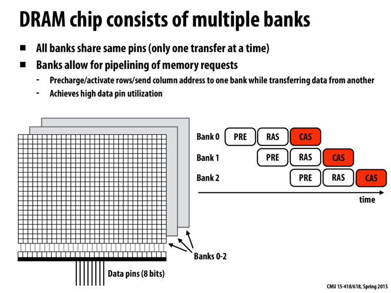
Is there any reason why "all banks share same pins"? Is it because that a coherence protocol on a "multi-pin" memory bank would introduce too much overhead?
kayvonf
Coherence serves to keep multiple copies of a single piece of information up to date when one of those copies is changes. Thus, coherence is not a relevant idea here.
There's only so many wires connecting to a DRAM chip. If you want more pin bandwidth, you add chips, which we do on the next slide. Banking is a technique to make sure a DRAM chip best utilizes the pins it has.
andrewwuan
@kayvonf Thanks for the reply! The reason why I was thinking about coherence protocol is that, if we have two pins that can read/write the same chip, and they each has something like a write buffer, then coherence problems may occur. But having multiple chip to increase bandwidth is definitely a simpler way to go!
vrazdan
Do all banks in the same chip store the same data? If they don't, how can you actually gain any performance benefit by pre-queuing requests (or, how is it any different than just having more chips)? If they do, how are all banks kept in sync whenever there is a data write, considering they're in different stages of their pipelines?
dumbo_
I think banks in same chip store different data. The data storage area is divided into several banks, so that the chip can work on several memory access commands at a time, interleaved among the separate banks. Say, if you want to read three lines and they are stored in different banks, you can pipeline PRE RAS CAS as in the slide, which allows higher data access rates.
afa4
I have the same question: Do all the banks in a chip store the same data?
mingf
They do not store the same data. The idea is that when one bank is performing precharging, another bank can perform activation. By pipelining like this, the chip can keep the data pins busy, which improve the utilization of the data pins.
kayvonf
@mingf is correct. The idea of memory banking is to overlap precharge/etc of one bank with data transfer from another. A read command to DRAM will access (bank, row, column).
regi
Is it the case that PRE/RAS/CAS have approximately the same latency? Otherwise, the pipeline may not be so tidy as depicted.
In other words, if a processor requests vars A, B, and C from DRAM and each var resides in a different bank on the same chip, we can be delivering A while row-activating B and pre-charging C.
rokislt10
In one of my other classes, 18-240 (Design and Structure of Digital Systems), we discussed hardware implementations of memory using tri-state drivers and shared busses. Both of the lectures, presented individually, left me a little lost but now that I have a good view from both a systems and hardware perspective, I understand the need for more memory banks much better.
Is there any reason why "all banks share same pins"? Is it because that a coherence protocol on a "multi-pin" memory bank would introduce too much overhead?
Coherence serves to keep multiple copies of a single piece of information up to date when one of those copies is changes. Thus, coherence is not a relevant idea here.
There's only so many wires connecting to a DRAM chip. If you want more pin bandwidth, you add chips, which we do on the next slide. Banking is a technique to make sure a DRAM chip best utilizes the pins it has.
@kayvonf Thanks for the reply! The reason why I was thinking about coherence protocol is that, if we have two pins that can read/write the same chip, and they each has something like a write buffer, then coherence problems may occur. But having multiple chip to increase bandwidth is definitely a simpler way to go!
Do all banks in the same chip store the same data? If they don't, how can you actually gain any performance benefit by pre-queuing requests (or, how is it any different than just having more chips)? If they do, how are all banks kept in sync whenever there is a data write, considering they're in different stages of their pipelines?
I think banks in same chip store different data. The data storage area is divided into several banks, so that the chip can work on several memory access commands at a time, interleaved among the separate banks. Say, if you want to read three lines and they are stored in different banks, you can pipeline PRE RAS CAS as in the slide, which allows higher data access rates.
I have the same question: Do all the banks in a chip store the same data?
They do not store the same data. The idea is that when one bank is performing precharging, another bank can perform activation. By pipelining like this, the chip can keep the data pins busy, which improve the utilization of the data pins.
@mingf is correct. The idea of memory banking is to overlap precharge/etc of one bank with data transfer from another. A read command to DRAM will access (bank, row, column).
Is it the case that PRE/RAS/CAS have approximately the same latency? Otherwise, the pipeline may not be so tidy as depicted.
@regi I think so http://15418.courses.cs.cmu.edu/spring2015/lecture/memory/slide_008
In other words, if a processor requests vars A, B, and C from DRAM and each var resides in a different bank on the same chip, we can be delivering A while row-activating B and pre-charging C.
In one of my other classes, 18-240 (Design and Structure of Digital Systems), we discussed hardware implementations of memory using tri-state drivers and shared busses. Both of the lectures, presented individually, left me a little lost but now that I have a good view from both a systems and hardware perspective, I understand the need for more memory banks much better.