So 16 x 64 x 32 = 32,768 CUDA threads can be live on the chip at once.
Any CUDA kernel launch that does not create at least 32,768 CUDA threads (and, in practice, some reasonable multiple of this number) will not be able to execute on the chip with maximal latency-hiding ability. Of course, if a program has high arithmetic intensity, then it will not need as many warps to hide latency.
yikesaiting
I can explain the calculation here. The first 2 lines are easy to understand. The third line means that on every core, because there are 64 warps, each with 32 SIMD units, a block with 128 CUDA threads needs 4 blocks. 64/4=16 blocks can be supported on one core. Thus, it is 16 * 128 = 2048 SIMD ALUs.
The fourth line means every core supports 64 warps. In total, 16 * 64 = 1024 warps can be supported. Each warp has 32 threads. Thus, there can be 32 * 1024 = 32,768 CUDA threads per chip.
kayvonf
@yikesaiting: Good job, but one correction. Perhaps you can update?
The third line is pointing out that there are 16 SMM cores per chip and that each of those cores as 128 total multiply-add execution units. (The line is about a property of the chip, not a property of a program run on it.)
Everything else is correct!
Hil
TFLOPS is the acronym for trillion floating-point operations per second.
Why is the double precision GFLOPS so drastically low? Is it a property of 32 wide SIMD?
kayvonf
"Shader processors" in NVIDIA speak are ALUs in my slides. Texture units and render output units are graphics-specific hardware functionality that applies to executing graphics-pipeline computations, not compute-mode operations, so we did not discuss them in class. (For those that are about to jump on me for the above statement, yes, I know it's possible to use the texture units from a CUDA program, but it's rare.)
It's clever marketing by NVIDIA to call ALUs "processors" since it sounds more sophisticated. For example, compare "2048 shader processors" in a GPU to a "4-core" Intel chip, that GPU sounds pretty good. Of course, if you count the ALUs in a modern quad-core Intel CPU you'd get:
4 cores x 8-wide SIMD x 2 SIMD units per core = 64 ALUs
CPUs are also clocked 2-3X higher than GPUs, so the actual peak compute difference is 2048/(64*3) ~ 10X. That's still a big difference, but not quite the same as 2048/4, which is what the people trying to sell NVIDIA chips would like you to think based on their terminology.
KyloRen
Is it then fair to say, that not all SMMs/shaders are available in compute mode? Since at least one SMM or atleast one shader will be provisioned for the more traditional GPU activities like UI drawings, other apps usage etc.?
Also what is the relative area of a shader vs. texture mappin vs renderer? Shaders seem to be the highest by an order of 20, is it possible to have more compute intensive GPUs (or rather just P(parallel)PUs?) with silicon area optimized with these "ALUs" and no extra paraphernalia?
https://en.wikipedia.org/wiki/Nvidia_Tesla <---?
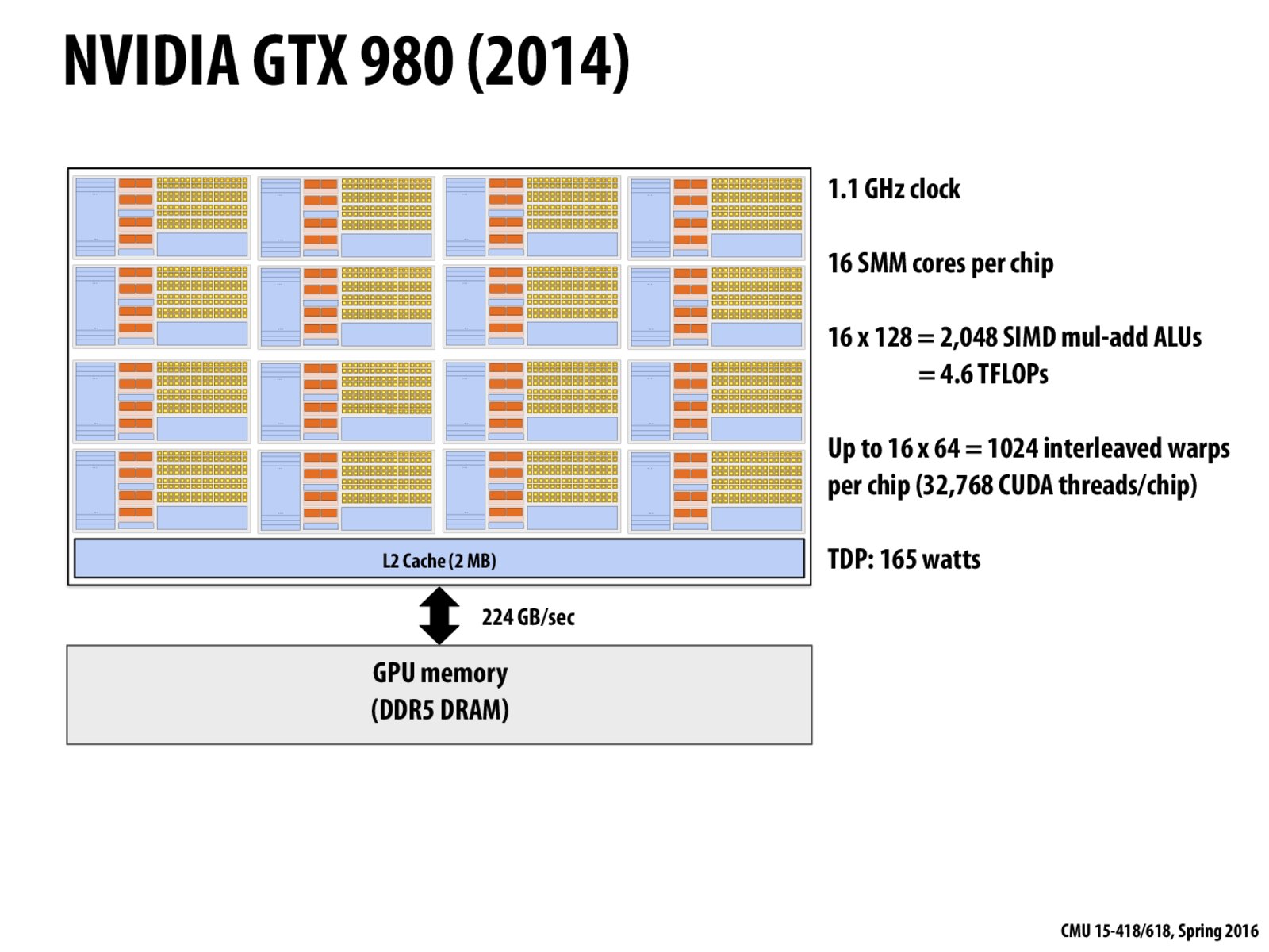
The geometry of the NVIDIA GTX 980 GPU is as follows:
In addition:
I can explain the calculation here. The first 2 lines are easy to understand. The third line means that on every core, because there are 64 warps, each with 32 SIMD units, a block with 128 CUDA threads needs 4 blocks. 64/4=16 blocks can be supported on one core. Thus, it is 16 * 128 = 2048 SIMD ALUs.
The fourth line means every core supports 64 warps. In total, 16 * 64 = 1024 warps can be supported. Each warp has 32 threads. Thus, there can be 32 * 1024 = 32,768 CUDA threads per chip.
@yikesaiting: Good job, but one correction. Perhaps you can update?
The third line is pointing out that there are 16 SMM cores per chip and that each of those cores as 128 total multiply-add execution units. (The line is about a property of the chip, not a property of a program run on it.)
Everything else is correct!
TFLOPS is the acronym for trillion floating-point operations per second.
@hil. Fixed.
Two questions: 1. How does the "Shader Processors : Texture mapping units : Render output units" as given here: https://en.wikipedia.org/wiki/GeForce_900_series map to the SMMs?
"Shader processors" in NVIDIA speak are ALUs in my slides. Texture units and render output units are graphics-specific hardware functionality that applies to executing graphics-pipeline computations, not compute-mode operations, so we did not discuss them in class. (For those that are about to jump on me for the above statement, yes, I know it's possible to use the texture units from a CUDA program, but it's rare.)
It's clever marketing by NVIDIA to call ALUs "processors" since it sounds more sophisticated. For example, compare "2048 shader processors" in a GPU to a "4-core" Intel chip, that GPU sounds pretty good. Of course, if you count the ALUs in a modern quad-core Intel CPU you'd get:
CPUs are also clocked 2-3X higher than GPUs, so the actual peak compute difference is
2048/(64*3) ~ 10X. That's still a big difference, but not quite the same as2048/4, which is what the people trying to sell NVIDIA chips would like you to think based on their terminology.Is it then fair to say, that not all SMMs/shaders are available in compute mode? Since at least one SMM or atleast one shader will be provisioned for the more traditional GPU activities like UI drawings, other apps usage etc.?
Also what is the relative area of a shader vs. texture mappin vs renderer? Shaders seem to be the highest by an order of 20, is it possible to have more compute intensive GPUs (or rather just P(parallel)PUs?) with silicon area optimized with these "ALUs" and no extra paraphernalia? https://en.wikipedia.org/wiki/Nvidia_Tesla <---?