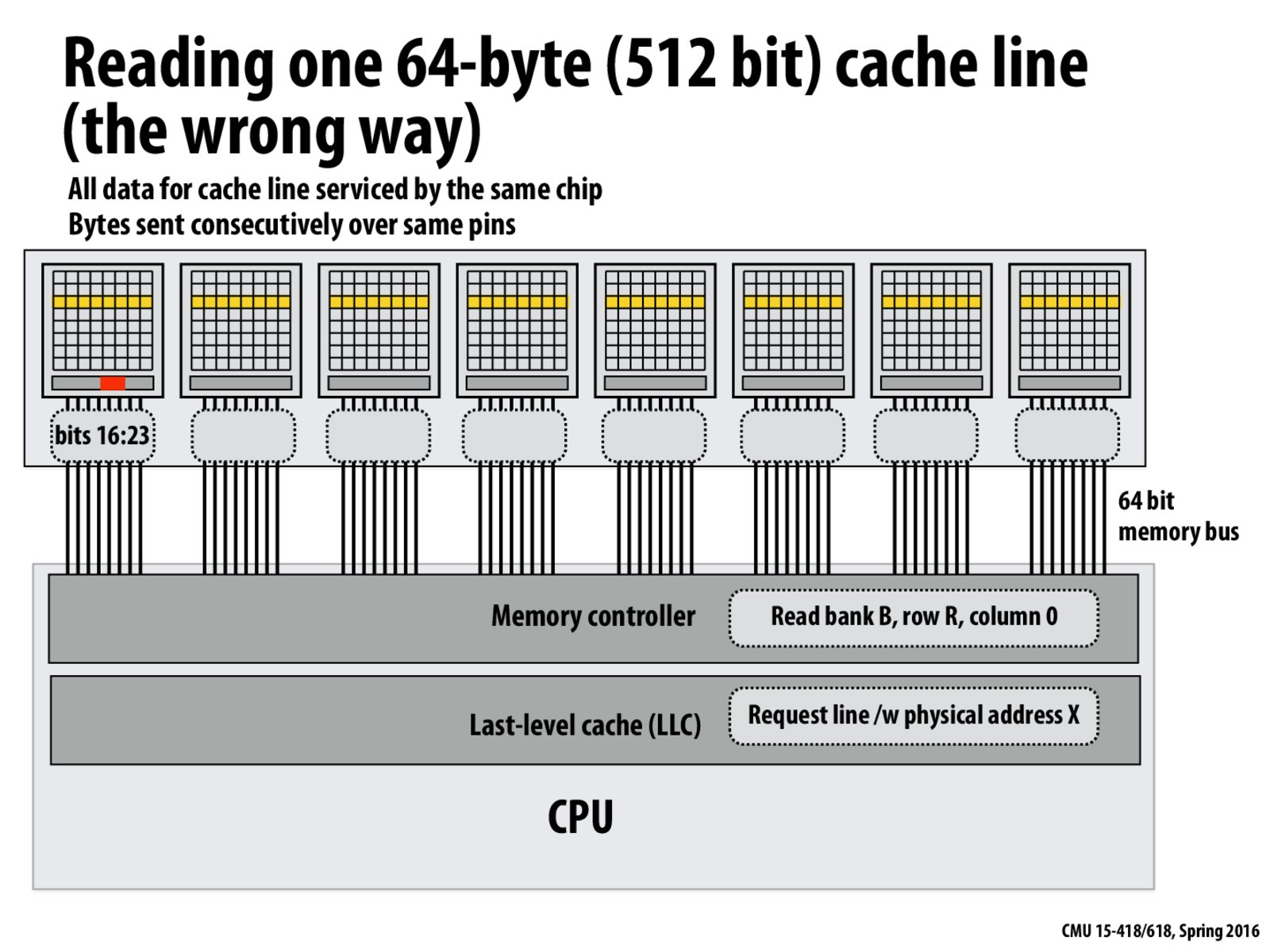
While we're able to read all the bits we need from the same row of one DRAM chip, we don't leverage our ability to read bits over the pins of the other DRAM chips at the same time. So while initially, it may have seemed like a good idea to map contiguous chunks of physical memory to the same row of the same chip in the DIMM, we see in the next few slides that it's actually more advantageous to map the contiguous blocks of memory in an interleaved manner across all the chips of memory, allowing us to achieve maximum throughput over all 8 sets of pins.
CaptainBlueBear
@kipper according to slides 16 and 17, the blocks in the graphics represent separate DRAM chips not banks. A DIMM is a collection of multiple DRAM chips each with its own data pins and then each chip has multiple banks (but the banks share the chip's data pins)
kipper
@CaptainBlueBear Oh yeah, you're totally right. Thanks for pointing that out!
While we're able to read all the bits we need from the same row of one DRAM chip, we don't leverage our ability to read bits over the pins of the other DRAM chips at the same time. So while initially, it may have seemed like a good idea to map contiguous chunks of physical memory to the same row of the same chip in the DIMM, we see in the next few slides that it's actually more advantageous to map the contiguous blocks of memory in an interleaved manner across all the chips of memory, allowing us to achieve maximum throughput over all 8 sets of pins.
@kipper according to slides 16 and 17, the blocks in the graphics represent separate DRAM chips not banks. A DIMM is a collection of multiple DRAM chips each with its own data pins and then each chip has multiple banks (but the banks share the chip's data pins)
@CaptainBlueBear Oh yeah, you're totally right. Thanks for pointing that out!