


In this diagram for every access in the DRAM, the entire row is copied to the row buffer. Hence to optimize this memory controllers first reorganize the pending requests before servicing them. One way to reorganize is to service the requests that need data from the row currently in the row buffer.
This can also lead to the problem of starvation for some access patterns as some requests may never be served because of the rearrangement.
This comment was marked helpful 0 times.

I believe it was discussed during lecture that starvation would be very unlikely because DRAM requests occur only if a memory request misses the last level cache, and therefore, subsequent accesses to the same area of memory would be cached.
Given 8 DRAM chips and striped memory storage, a cache line would take $64 / 8 = 8~\text{bytes}$ in each chip, and because a row of the chip has $2048~\text{bits} = 256~\text{bytes}$, a row could be responsible for a maximum of $256 / 8 = 32~\text{cache lines}$. Therefore, in the worst case, some memory access could be delayed by 32 accesses, and most likely not much more than that because none of those 32 cache lines are likely to get evicted from the last level cache in the time it takes to read in all 32.
This comment was marked helpful 0 times.

Although unlikely it is possible to have starvation due to unfairness in the DRAM controller. This example was given in the first lecture of Professor Mutlu's 18447 course: given two threads running similar for loops reading/writing two large arrays, differing only in the sequential vs. random access of the arrays, the thread with the sequential access will be prioritized due to its high row buffer locality.
This comment was marked helpful 0 times.

This is also the motivation behind rearranging memory access, so that we minimize the number of times we need to copy rows into row buffers.
This comment was marked helpful 0 times.

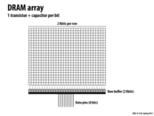
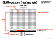
Row buffer can be thought of as a cache that holds only 2kb, we want to optimize our access pattern so that each time we load bytes we don't have to go through steps 1 and 2 on the previous slide.
This comment was marked helpful 0 times.
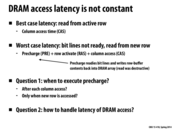

The advantage of precharging immediately after a request finished is that it improves the performance of the worst case. Since when a new request comes the charging has already been finished, we only need to wait for RAS and CAS. The drawback is that it destroys the data in the row buffer, which makes the "best" case only has the same performance with the other case. However, the precharging immediately policy may still be a good choice because of an assumption. It is reasonable to assume the DRAM access is almost random, since the access would first hit cache if there is any locality.
This comment was marked helpful 1 times.

I think there might be cases where there is much locality. For example if we have a loop over a bunch of data accesses, then the first round of cold misses would all hit memory, and they would have good locality. Also, there is the case where the working set of the loop is too big to fit in the cache. I think these cases probably happen more than we'd expect, which explains the structure of DRAM as described in the following slides.
This comment was marked helpful 0 times.
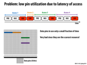

My understanding of this slide is that if you're just performing these memory accesses in sequence, if we have a lot of different rows being accessed then we're only using the data pins about a third of the time to read 8 bits. The rest of the time is spent waiting for the other steps, like pre-loading a row and putting the row into the row buffer. So, we need to try to use the pins more since they are the scarcest resource and the bandwidth bottleneck.
I'm confused about one thing though: I thought that generally you would always load up a whole cache line from memory at a time upon a cache miss. Why is it that these accesses are just 8 bits at a time, and then move on to different rows in DRAM? Or is it actually for this reason that we load a whole cache line from memory at a time, using the 8-chip mechanism described later?
This comment was marked helpful 0 times.

@arsenal: Correct. This slide is simply illustrating how DRAM works (what it's capabilities are).
In a real system, we are often only requesting cache line sized chunks of memory from the memory system, and that bulk granularity is key to enabling higher performance access to memory. Later in the lecture we talk about mapping cache lines to chips in a DIMM.
This comment was marked helpful 0 times.

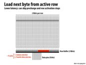
Could someone help me understand what is going in this slide (and last slide)? Based on my understanding, this slide shows that combining consecutive accesses to the same row into one access leads to lower latency. Is that a reasonable interpretation?
This comment was marked helpful 0 times.

My understanding is that our DRAM should just allow requests for more data than could be transferred out from the data pins in any one clock cycle in order to optimize our latency. So I think you're right, @tomshen.
This comment was marked helpful 0 times.

A system's bottleneck should never sit idly if one wants to maximize throughput. That's why each DRAM command describes bulk transfer. The controller gets more data than each request. The data pins are kept busy by loading the next lines that may be transferred, even if they don't end up getting used.
This comment was marked helpful 2 times.

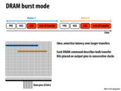
Burst Mode capability of DRAM allows it to skip one of the three following steps when transmitting data in a data transaction to increase data throughput: 1. Waiting for input from another device 2. Waiting for an internal process to terminate before continuing data transfer 3. Transmitting information which would be required for a complete transaction, but which is inherent in the use of burst mode.
This comment was marked helpful 0 times.

Every time fetching a cache line size of data from the memory to the cache can amortize the overhead cost.
This comment was marked helpful 0 times.
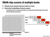

This is called bank-level parallelism. The main idea is to use multiple banks and pipeline the operations to achieve latency hiding. One problem is when requests are to the same bank, then the operations need to be serialized, cause bank conflict.
This comment was marked helpful 0 times.

Nevertheless, in that case (two requests to the same bank), we would handle the requests as if there were no banks. Basically having banks only makes the latency for a request better or the same then if there weren't banks. I can't imagine a situation where it could be worse.
This comment was marked helpful 0 times.

I think having too many banks might result in a constant bottleneck at the data pins, causing overall longer latency for DRAM accesses. The number of banks would probably have to be decided by statistical data/predictions for data access patterns.
This comment was marked helpful 0 times.

Having more banks means that we require a few input pins to choose the data bank. SDRAM is usually divided into 2, 4, or 8 banks (to best utilize 1, 2, and 3 bit inputs). In addition, I believe that since DRAM is much less expensive than SRAM, putting more banks on a chip doesn't significantly increase the overall cost of memory.
This comment was marked helpful 0 times.
@LilWaynesFather
The data pins are already the scarcest resource. Ideally, they should always be running. I think the number of banks shown here is probably what is the derived from "statistical data/predictions for data access patterns."
This comment was marked helpful 0 times.

I'm not sure if this was mentioned in the lecture but what are banks exactly?
This comment was marked helpful 0 times.

@elemental03 It is a logical unit of storage, but hardware-dependent. Could be something like a cache. Usually of medium size. http://en.wikipedia.org/wiki/Memory_bank
This comment was marked helpful 0 times.

Quick summary of the next few slides:
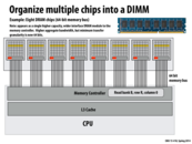
Memory is abstracted as one large "chunk" of consecutive memory, and programmers often think of it as a single chip. However, this is not completely true! RAM (in this case) is actually split across EIGHT chips (or nine, if parity is included). So how should the memory controller actually split up data across these eight chips? Should a group of local memory be stored on one chip, or on many chips? To maximize utility of the memory pins (a potential bottleneck), data is striped across many chips, so they can be accessed in parallel. In the slide above, we see this "stripe" of memory as a yellow line. In reality, the memory controller may be even more intelligent with data placement in RAM than a simple striping mechanism, to maximize throughput when accessing memory.
This comment was marked helpful 0 times.

We described the data pins in the single memory bank system as the bottleneck in the system, and I assume that more such pins were not put into the chip because they are monetarily expensive to mass produce or such. If so, what advantage are we gaining from a 8 bank memory system with 64 data pins vs one memory bank 8 times as large with 64 pins as well.
From my reasoning, there would still be a transfer granularity of 64 bits, the memory bandwidth would be increased the same, and better yet the recharge mechanism of such a system would not have to be copied over 8 different memory banks, potentially saving power.
Am I missing something here; how does parallelizing the memory across multiple banks advantage the system when the bottleneck comes from the number of data pins in the system, a variable that can be increased without splitting up the memory banks. The only thin I see is that a parallel model conserves surface area (by being able to stack banks).
This comment was marked helpful 0 times.
And just for the curious, this lecture only deals with the chips on one side of a DIMM. The D in DIMM is for "dual" and there's another set of chips on the other side of the module. (not shown in the picture). Of course, if you open up a modern machine you'll see multiple DIMMs as well.
This comment was marked helpful 1 times.

@vrkrishn That would require a single giant IC with 64 pins instead of 8 ICs, which seems harder to fit onto a circuit board and makes manufacturing more difficult (having more and smaller chips allows defective chips to be replaced more easily). It seems to me that pins are expensive not so much because they're hard to manufacture as because of the space they take up.
This comment was marked helpful 0 times.

According to this (old?) arstechnica article, increasing the pin count not only increases the cost of manufacturing memory, but also the cost of any connectors and also the motherboard connected to the memory. So increasing the pin count will increase the cost of several parts of the system.
This comment was marked helpful 0 times.
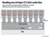

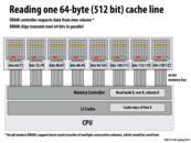
In class, Kayvon also talked about putting one 64-byte cache line in one DRAM chip. Although it might utilize "burst" reading mode of the DRAM chip, we would get almost 1/8 performance because we need to use 8bit memory bus 8 times.
This comment was marked helpful 0 times.
@taegyunk Wait I'm confused on what your saying - what would the point of a 64-byte cache line in a DRAM chip be. When there is a cache miss and memory is requested from the DRAM, 64 bytes would be requested to fill the cache line. So we would have the "burst" read, get 64 bits at a time, have to make 8 requests to get all 64-bytes, but then, this data would already be in the cache, so there would be no need to keep that data in the DRAM.
This comment was marked helpful 0 times.

@ycp , @taegyunk is talking about how the data is spread over the 8 DRAM chips to ensure that the 64 memory bit bus on ALL 8 DRAM chips always have enough work. And not all work is done by the same DRAM chip.
This comment was marked helpful 0 times.

@ycp Just to expand a little on @shabnam's explanation. If an entire cache line were to be placed in 1 DRAM chip, the throughput would be limited to 8bits/cycle (despite the presence of burst mode) since one DRAM can only serve out 8 bits per cycle. However, if a cache line were to be placed across 8 DRAM chips, although we won't be able to utilize burst mode, the throughput would be 8*8bits/cycle since we can utilize pins to all memory chips to serve the request (versus just 1).
This comment was marked helpful 0 times.
To clarify, even with byte interleaving across the DRAMS you can utilize burst mode transfer. Consider a cache line of size 64 bytes (512 bits). Only 64 bits comes in each cycle as shown above, so there's still 8 consecutive bytes in each DRAM chip row that needs to be transferred.
This comment was marked helpful 0 times.
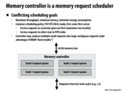
The trade-off of FR-FCFS is starvation. For example, image a scene where one coming request, R, is not in DRAM buffer, while there are many hit-buffer requests coming continuously. A controller following the FR policy would always choose the other requests to maximize throughput. But in the view of request R, it sees an extremely long latency. While it may be acceptable for throughput-optimizing system, like GPU, this unfairness is intolerable for CPU for the seek of quality of service. As a result, CPU often has a more complicated scheduling policy.
This comment was marked helpful 0 times.

Is starvation not limited by a buffer simply not being able to hold that much? 2KB may seem like a lot but if requests are generally 64 bytes (cacheline size), you would only have 32 hits (at most? perhaps not if some terrible caching caused evictions each time). Even if the DRAM were to cut off accesses after 32 hits (wouldn't be hard, I imagine), I feel like everything would be pretty smooth. What makes the policy unacceptable for a CPU? I may be thinking about these timings very naively.
This comment was marked helpful 0 times.
One example:
http://users.ece.cmu.edu/~omutlu/pub/tcm_micro10.pdf
This comment was marked helpful 0 times.
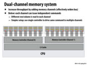

Since it is a simpler setup to use a single controller to give the same command to multiple DRAM channels, this seems like an argument in favor of putting one cache line across the same row of multiple channels. Usually when memory is accessed the program requests a whole cache line, so to avoid bottleneck (as discussed in previous slides), it will have to send a request to multiple DRAM channels (in this case 8). If the cache line is mapped to the same row across all 8 channels, then the memory controller only needs to issue one request and duplicate it 8 times. This would be more efficient than if it had to issue 8 different requests because the cache line was spread out on different rows across the channels.
This comment was marked helpful 0 times.
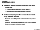

A little recap on the hierarchy of DRAM: down the lowest level you have a row of transistors that connect to capacitors used to records bits. To access a set of 8 bits (specific number depends on system), you need a CAS (column access strobe). When you have multiple rows, you have a bank. To access a particular row, you need a RAS (row access strobe). Then going a little up, multiple banks that shares the same data pin is a chip. And a modern DRAM usually has multiple chips on both side of the hardware, which is a DIMM (duel in-line memory module). Each DIMM interacts with one memory controller, which connects to the memory bus to the rest of the system.
This comment was marked helpful 0 times.

One of the stuff mentioned in lecture is that memory controlled will respond to CPU request faster than GPU because GPU has more threads to hide latency while CPU would stall quickly if requested memory does not get back asap.
This comment was marked helpful 0 times.


As someone who doesn't know very much about computer architecture, please excuse my ignorance, but why can't all of memory + CPU be located on the same chip? Does it cost more/ use more power/ etc? Why are buses used in the first place?
This comment was marked helpful 0 times.

@sbly: This actually has been explored: Computational RAM. The linked article suggests that the purpose of the various PIM (processor-in-memory) projects, the most notable of which was the Berkeley IRAM project, was to reduce memory latency and increase throughput. The main reason that it is difficult to put DRAM but not SRAM on the same chip as the processor is that the microprocessor technology for CPU chips optimizes for speed whereas DRAM chips optimize for density. SRAM can be built in the same way as the microprocessor technology, so it can more easily be put on the same chip.
This comment was marked helpful 0 times.
Another more non-technical reason for why everything isn't located on the same chip is that many times buyers want modularity. If everything is on the same chip, if one part breaks, you have to replace the whole chip. If you want to upgrade just the memory/processor, you'd have to replace the whole chip. For supercomputers this would be a huge hassle. So they why not just fit tons of memory onto the same chip? Then the chip will probably get so large that you'll end up having the same issues that you did before with large distances between the processor and the memory.
This comment was marked helpful 0 times.

System-on-a-chip architectures try to implement this too. It's kind of interesting to see how ARM architectures like the mobile devices take advantage of this, especially when physical space is precious.
This comment was marked helpful 0 times.
(Another person who knows little about computer architecture here) Would heat generation also be a problem? If you put more components that generate heat closer together, I'd imagine that the amount of heat would grow to the point that you would also have to design a way to remove the extra heat generated as a result of putting the components closer together.
This comment was marked helpful 0 times.
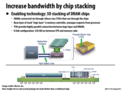
This seems to offer a lot of benefits without much drawback. Can someone clarify why this isn't almost always used? Would heat/power consumption be the issue?
This comment was marked helpful 0 times.
3D stacking is emerging technology that you'll likely see used more and more often for high performance systems in the coming years.
This comment was marked helpful 0 times.

I was thinking that why DRAM can't adopt the architecture like disk. 8 plates construct a cylinder, then one controller can control all the plates. DRAM can also let 8 banks be a group, and have 8 groups, as data request a always larger than 64*8 bits, I suppose it will have a big improvement.
This comment was marked helpful 0 times.

@black I feel like the architecture of hard disks (SATA) is more like a compromise than a feature since the plates have to spin and pin has to locate data... and a cylinder would occupy more spaces than a chip. And now days Solid State Disks are more and more popular since they are faster and smaller, the architecture of disks is more and more like a DRAM :)
This comment was marked helpful 0 times.
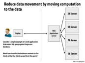

The result of the query is much smaller than the database contents needed to perform the query, so it is more efficient to copy the result to the client (not to mention all of the security concerns with giving the client the full database).
This comment was marked helpful 0 times.
I think one more thing to reduce the data movement is to cache query result on the client-side.
This comment was marked helpful 0 times.
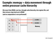
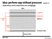

In this slide we see how memcpy can be performed entirely in memory. Rather than transfer each byte from memory to the processor and back, every DRAM line can be read into the row buffer and written back twice, once to the original row and again to the target row. This results in an effective copy rate thousands of times the original.
Given current memory architecture this would require memory to be copied in 16 Kb chunks aligned to 16 Kb since we can't just copy part of a row. In order to support smaller or unaligned copies, the memory could be built to have some sort of mask which allows partial rows to be written back.
This comment was marked helpful 0 times.

How much is this technique used in current hardware?
This comment was marked helpful 0 times.

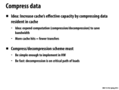
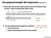
Summary of the next few slides: Another way to deal with data transfer being the bottleneck is to compress data so we can save bandwidth. This scheme has to be simple and fast for the reasons listed above. One way to compress is use the fact that nearby data probably has similar values. Hence, we select the minimum or the first value in the line as the base and record the others in the cache line by deltas (original value - base). However, the result will be obviously bad for nearby data that deviates a lot from each other. Hence, we use a two pass basing. We first compress with zero as the default base (which we do not have to store, but do not compress the value if zero is a bad base for the value. Now, in the second pass, out of those uncompressed values, we select the first one and use that as the base for all other uncompressed values.
This comment was marked helpful 0 times.

To clarify, the line about "more cache hits = fewer transfers" suggests that because the cache's effective capacity is increased and more data fits in the cache, there will be overall fewer cache misses and more cache hits as fewer cache items are evicted. This means that there will be fewer full transfers because the cache can be used more often. Ideally, this savings in transfer time and cost would offset the additional cost to compress and decompress the data.
This comment was marked helpful 0 times.

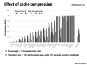
I found the paper about this compression scheme here. It has an interesting analysis of performance improvements, as well as an explanation of how it's actually implemented.
This comment was marked helpful 1 times.

In the paper they imply that cache compression adds hardware complexity. But it's not clear to me whom exactly performs the compression and decompression. Is it the processor, or a specialized harware device?
This comment was marked helpful 0 times.
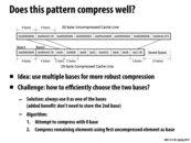
I am very curious, so we do need to store meta data for each of the values right? (e.g., which base, number of bytes used, etc.) Is it still worth it to do the compression?
This comment was marked helpful 0 times.

It seems that (and the paper suggested a few slides earlier) the number of bytes used in compression is different for each base, so those that are compressed to 1 byte goes to base 1, those compressed to 2 bytes go to base 2, etc., so the corresponding compression values for each base don't need to be stored. Otherwise, each pattern in the cache line can probably have start / end tags. From this you can infer the size of the compression, and thus the base that was used.
This comment was marked helpful 0 times.

Interesting that the peaks happen at 2 bases for almost every test, and occasionally at 3. This suggests that the overhead of using many bases is rarely worthwhile, and generally nearby data is similar to only a couple of different values.
This comment was marked helpful 0 times.

In this slide, we see the birds trying to take back their eggs by flinging themselves haphazardly at the pigs. However, they are only using one slingshot, which causes a bottleneck in bird-throughput. They could parallelize their self-sacrificing escapades by setting up multiple, independent slingshots (in which case they would have to coordinate their efforts through carrier pigeons), or by putting multiple rubber-bands on the same slingshot and launching many birds at a time, which I call SSMB - single slingshot, multiple birds (not to be confused with the viral internet video two-birds/one-slingshot). A SSMB width of four seems optimal in this situation.
This comment was marked helpful 6 times.
In most applications many frame tiles do not change, so we can use this property to reduce the number of GPU writes by not rendering that tile if it is not going to change For example: Here in the first picture the sky is not going to change frequently. This leads to energy savings.
This comment was marked helpful 0 times.

Although unlikely, it is possible for hash collisions to occur. If that happened, the system would mistakenly think that a tile hasn't changed and wouldn't redraw it, when actually it has changed and should be updated. The result would be a graphical glitch in the scene until the tile is updated again later. As mentioned in class though, this really isn't a big deal for a couple of reasons:
- It's highly improbable and won't happen frequently
- It's a minor artifact, affecting only a single tile and lasting only a moment
- In the case of a smoothly changing scene, the old and new tiles may be visually similar anyway
In summary, a hash collision may happen on occasion in one tile for one frame, but it will probably be imperceptible, or at worst be a minor artifact. The benefit in bandwidth savings greatly outweighs the potential drawback of the occasional hash collision.
This comment was marked helpful 0 times.

Another practical implementation of memory compression for GPUs is for the frame buffer. Intel GPUs support "framebuffer compression." The observation is that parts of the screen have a contiguous color, and that most regions of the screen do not update very often. To take advantage of this, framebuffer compression uses run-length encoding to compress each row in the framebuffer (this is the same compression scheme GIFs use). As rows on the screen change, the compressed version of the modified row is not an accurate representation of the actual row, so the GPU uses the uncompressed copy of the row to draw that row on the screen. Otherwise, the GPU uses the compressed version, saving bandwidth, and thus energy. When too many rows have changed, the GPU recompresses the entire framebuffer and all compressesed rows are valid again.
This comment was marked helpful 0 times.

DRAM is made up of rows of capacitors that either hold a charge, or do not. A capacitor of this kind is only capable of reliably holding a charge for about 50ms. This means that rows have to be recharged frequently. This is done the same way a read or write would happen. The row that is to be refreshed is pulled down into the row buffer, and then it is written back. More information about memory refreshing.
This adds complexity to the scheduling the memory controller must do. It must interleave actual memory accesses with refreshes of DRAM cells properly. It must schedule the use of the row buffer so that no row ever is at risk of becoming corrupted (ie. have bits flipped due to capacitor draining).
This comment was marked helpful 0 times.
This is as opposed to SRAM (static RAM), which holds charge as long as power is being provided to the transistors. SRAM is hence able to have lower latencies and less power consumption since it doesn't need to interleave refreshing operations with actual memory accesses. However, this functionality requires packing additional transistors into the chip - 6 per bit as opposed to the single transistor-capacitor pair of DRAM - which makes SRAM the more expensive alternative, and is part of the reason DRAM is usually the choice for implementing main memory.
This comment was marked helpful 0 times.
There is research into new types of RAM such as MRAM, which is magnetic RAM and is non-volatile, so no refresh is required and no power is needed to retain the contents. This has implications for instant hibernation and power management.
This comment was marked helpful 0 times.